Einar Abell
EDN
This Design Idea shows how to add positive feedback to a Darlington pair to create a Schmitt trigger with very high current gain (typically 10,000). I don't know of any similar circuits to compare this to except ICs. However, it performs a very common function in a very simple manner. The circuit can be designed to handle load currents in the range of milliamps to amperes, with input impedance above 100 MΩ for lower load currents.
 |
|
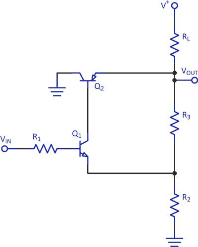
| Figure 1. | Two-transistor Schmitt trigger. |
Figure 1 shows the basic circuit in its 'NPN', active low version, and Figure 2 shows the 'PNP', active high version. R2 and R3 create a voltage (through RL) at Q1's emitter. As the input voltage increases from zero to the VON point given by Equation 1, Q1 starts to turn on. Its collector current will be amplified by Q2, pulling down VOUT, which will reduce the voltage at Q1's emitter, turning it on more. This process will continue until Q1 is saturated, assuming the positive feedback from R3 is greater than the negative feedback caused by the current from Q1's emitter.
| (1) |
Equation 2 describes this situation; the equation should satisfied by at least a factor of two. The greater the inequality, the greater the amount of hysteresis. Eq. 2 can be solved to give limits to the circuit elements as shown in Eq. 3 for RL, and Eq. 4 for RIN (a.k.a. R1). Eq. 4 and Eq. 5 also give the limit for R3, which must be less than RL times the gain of Q2 to keep RIN a positive value; typically R3 will be one half or less of this amount. Obviously, it helps if Q2 is a high gain part. Choosing R3 (and VON) allows calculation of R2 with Eq. 6.
 |
(2) |
| (3) |
 |
(4) |
| (5) |
| (6) |
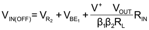
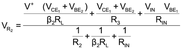
In the 'on' state, VOUT is approximated with Eq. 7. Because the dominant term depends on the gain of Q2, the measured voltage is usually somewhat different, but is typically in the 2 to 3 volt range. The current in RIN also adds into the voltage on R2 (Eq. 9), and if R1 is too small, the current will significantly increase VR2 (in fact, if RIN is zero, VOUT will follow VIN). As the input voltage drops, the output will stay on until Q1 comes out of saturation. At this point, the positive feedback will turn both Q1 and Q2 off. Eq. 8 describes this VOFF point.
 |
|
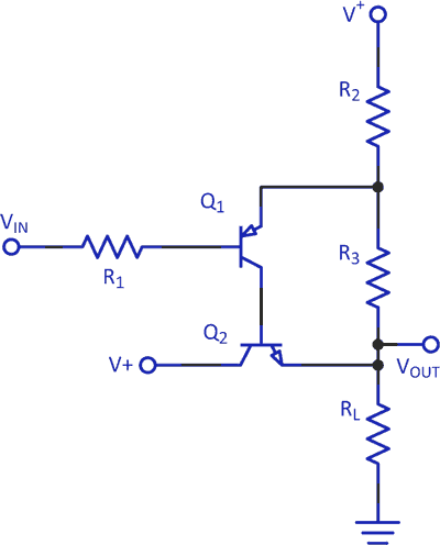
| Figure 2. | Active-high version. |
Since you will usually want to keep R2 at a minimum to keep VOUT low, adjusting VOFF will rely on varying R1, but again, this VOFF value is dependent on the betas of Q1 and Q2.
| (7) |
 |
(8) |
 |
(9) |
With
![]()
and
![]()
This loosely defined turn-off point is one of the shortcomings of this circuit. However there are still plenty of applications that don't need precisely defined trip points. Generally, you would select R2 and R3 to be as low as practical, keeping in mind quiescent current flows through RL, and make R1 as large as needed (or allowed by Eq. 4), and be satisfied with whatever VOFF you end up with. The other main shortcoming is the relatively high voltage on Q2 when it is conducting, making it impractical for currents above a few amperes. This also limits the circuit to higher V+ voltages, making its niche use at higher currents and voltages than that of most ICs.
 |
|
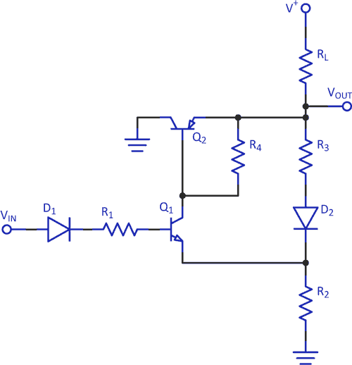
| Figure 3. | Practical component additions. |
Figure 3 is Figure 1 redrawn to include three extra components that will be used in many applications. D1 prevents breakdown of the Q1 base-emitter junction if the voltage at the emitter should exceed 6 to 7 volts while in the off state. D2 reduces the contribution of R3 to the on-state output voltage. D2 is especially important if you make R3 equal or less than R2. R4 improves turn off of Q2 and keeps it from tripping on leakage current from Q1.
Q2 may be Darlington transistor (there seems to be little advantage to making Q1 a Darlington). Alternately, either or both transistors may be MOSFETs (with appropriate changes to the equations).