By combining charge-pump ICs with additional discrete components, this inverting design produces a negative output from a positive one with lower ripple and output impedance.
An inverting charge pump takes a positive supply voltage and generates a negative supply from it. Discrete-design charge pumps can offer reduced output impedance, reduced output-ripple voltage, controlled charging currents, and higher working voltages compared to IC-only pumps. The 15-V supply level shown is not handled by presently available ICs, but it has always been an objective to include ICs for cost reasons. This circuit is a step toward that goal.
 |
|
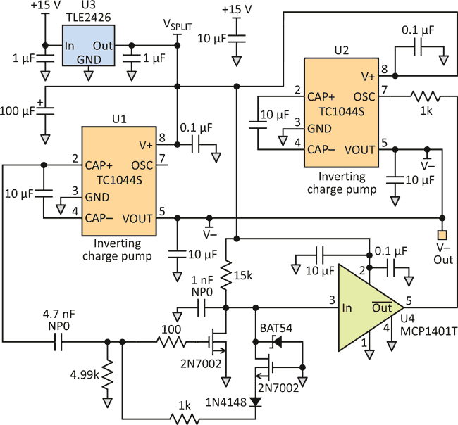
| Figure 1. | The inverting charge pump combines a pair of charge-pump ICs with a separate MOSFET-based detector/clock-doubler subcircuit, which in turn enables synchronization and enhances performance. |
The discrete-based capacitive charge pumps here use synchronously timed dual-pump capacitors and work at voltages to +15 V dc. The circuit (Fig. 1) contains an edge-detector/clock-doubler subcircuit which was separately simulated and validated via a Spice model (Fig. 2).
 |
|
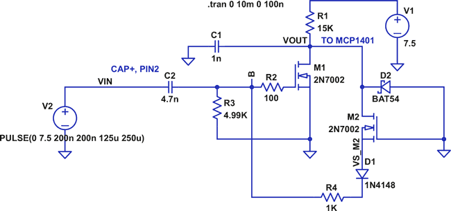
| Figure 2. | In this LTSpice simulator schematic for the edge detector/clock doubler,M1 detects rising VIN edges and M2 detects falling VIN edges. |
Charge pumps U1 and U2 (Microchip Technology) have a maximum input-voltage rating of 12 V dc, which is close to the desired 15-V dc rail. U3 takes the positive supply and divides it by half, to reduce it to an acceptable input-voltage level for U1. U1 and U2 are set up in a standard inverting configuration. Each has its own pump capacitor (CAP+ to CAP–) and hold capacitor (V– to GND). An additional circuit with two 2N7002 and MCP1401T devices creates an out-of-phase clock for the U2’s pump capacitor, to allow for synchronous pumping on each half-cycle of the capacitors.
In the edge-detector subcircuit, the rising edge of VIN to C2 produces the drain current for MOSFET M1, and the falling edge of VIN produces the drain current for M2. The drain currents are in parallel and produce an output voltage to 7.5 V through R1. U4 is used as a level shifter to shift to the supply voltage level of U1 and U2, and this signal is fed back to the oscillator input of U2. The signal from U1’s charging capacitor is doubled to account for the divide-by-two circuit. Compare this synchronous design to Figure 4 of the TC1044S datasheet, “Paralleling Devices Lowers Output Impedance,” which shows each TC1044S feeding its charge to the hold capacitor, but with random timing.
The TC1044S has a timing resistor for tuning pump frequency, which makes it possible to lower the charge pump’s frequency. Doing so requires a capacitor between pin 7 and the ground of master pump U1. Lower frequencies require larger pump/hold capacitors, but make the post-regulation circuit easier to implement because the bandwidth of the regulator IC is typically lower in frequency. Pump frequencies in the kilohertz range can exceed the voltage-regulator bandwidth.
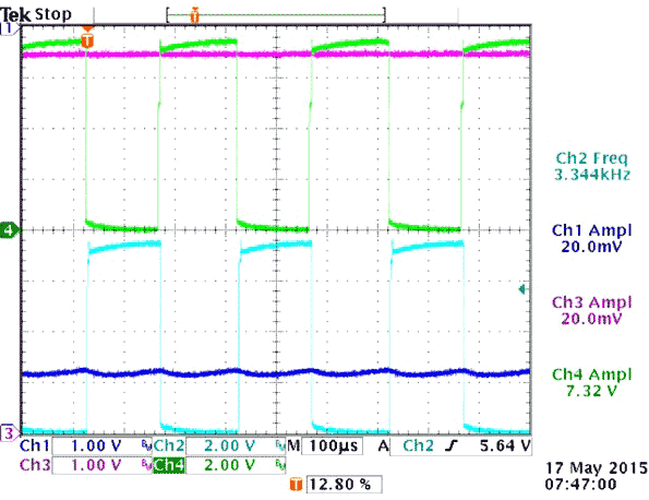
The oscilloscope photo shows four key waveforms with an output load of 200 Ω (Fig. 3). Note how pump-charging signals CH2 and CH4 are 180° out of phase. While one pump capacitor is charging, the other is sourcing charge to the hold capacitor. CH1 shows the effect of bringing a fully charged pump capacitor to the hold capacitor on each half cycle. The ripple-voltage trace tracks the pump capacitors being applied in sequential order to the hold capacitor. CH3 shows that the voltage ripple on the rail splitter is minimal, even when charging each 10-µF pump capacitor; this is due to the 100-µF tantalum capacitor on the output of U3.
 |
|
| Figure 3. | This four-channel oscilloscope screen shows performance in detail, with V– driving a grounded 200-Ω load. CH1 is V–; CH2 is pin 2 of U1; CH3 is split voltage VSPLIT at 7.5 V; and CH4 is pin 2 of U2. CH2 and CH3 share the same baseline. |
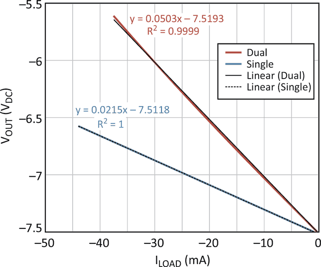
The load line (Fig. 4) was plotted by varying RLOAD with a decade-resistor box and recording the output voltage, and ILOAD was calculated as VOUT/RLOAD. The slope of the load line is the dc output impedance (ohms). The output impedance for dual-pump design is 21.5 Ω, compared to 50.3 Ω for the single-pump approach. A portion of the output impedance is due to the on-resistance of the switching MOSFETs in U1 and U2, which are used in series with the pump/hold capacitors. These can’t be changed unless a discrete circuit design is used.
 |
|
| Figure 4. | The output impedance ZOUT difference is less than 1:2 as seen in measured data of the dual-pump capacitor version (21.5 Ω) versus the standard single-pump capacitor version (50.3 Ω). |
Peak-to-peak ripple voltage of the charge-pump output for both single and dual versions was also measured. For an output voltage of –6.6 V dc, the dual-version ripple was just 180 mVP-P, while the single pump showed ripple of 550 mVP-P.