Contemporary power supplies use switching techniques to achieve the desired output voltage from the primary source. Switching power supplies, however, are often too noisy to be used in sensitive analog circuits. You may find linear power supplies to be preferable in these cases.
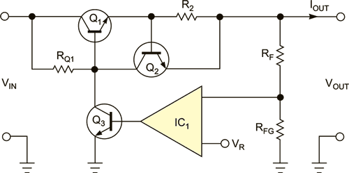
A standard practice for a linear voltage regulator is shown in Figure 1. A higher-than-desired, unstable voltage is connected to the input, VIN, and the series-pass transistor, Q1, reduces the voltage to the desired level at output VOUT. An error amplifier, IC1, compares a fraction of VOUT with a reference voltage, VR, and controls Q1 to keep the output fixed regardless of the load current, IOUT, and variations of VIN. Such a circuit is suitable only for a small range of output voltages.
 |
|
| Figure 1. | A standard linear voltage regulator connects the feedback directly to the series-pass transistor, Q1. |
When a wide range of output settings is desired, as in laboratory power supplies, the value of resistor RQ1 must be small enough to allow sufficient base current for transistor Q1 at the high end of the output voltage range, but excessive power is dissipated at this resistor and transistor Q3 when output voltage is reduced. Additionally, Q3 must withstand the maximum VIN.
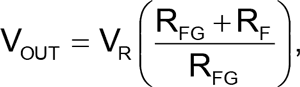
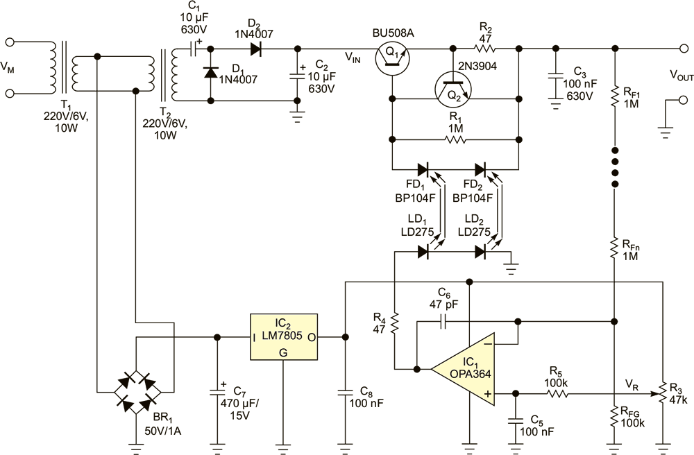
You can use the circuit in Figure 2 to overcome these problems. Two standard transformers, T1 and T2 (220 V ac to 6 V ac, 10 W), are used to make an isolated replica of the mains supply, VM. This replica is doubled and rectified using D1, D2, C1, and C2 to get about 560 V at VIN from 220 V ac at VM. As in the standard Figure 1 connection, a series-pass transistor, Q1 (BU508A), is used to reduce the unstable VIN down to a fixed VOUT, and IC1 compares the divided VOUT with VR. Potentiometer R3 sets VR to allow for the adjustment of VOUT, as given by the following equation:
where RF = RF1 + RF2 … RFn.
With 10 resistors (1 MΩ each) connected in series to form RF and a maximum reference voltage of 5 V, the output voltage can be set from 0 to 505 V. The OPA364 operational amplifier is a rail-to-rail input type to allow proper operation, with VR ranging from 0 to 5 V, and is able to source a current of up to 40 mA.
 |
|
| Figure 2. | Optical coupling isolates the high voltage at Q1 from the op-amp output. |
To reduce the power dissipation caused by driving a series-pass transistor and expand the output voltage range, the driving of transistor Q1 is done in an unconventional way using optical isolation. Two photodiodes, FD1 and FD2, operating in photovoltaic mode, provide the driving current for the base of transistor Q1. Light falling on the photodiodes causes a current flow into the base of Q1.
The maximum voltage from a single photodiode working in photovoltaic mode is not sufficient to drive the base; therefore, two photodiodes are connected in series. Photodiodes for infrared light at 870 to 950 nm are used, and two IR LEDs, LD1 and LD2, illuminate them. The LEDs are standard 5-mm, plastic-encapsulated types. To improve the transfer ratio of the current through the LED versus the current generated by the photodiode, cut off the tops of the LEDs and polish them to form a flat surface. Place the photodiodes in proximity to the surfaces obtained. The transfer ratio of this homemade optocoupler is about 0.05. (The current of 20 mA through the LED causes a current of 1 mA through the photodiode.) Alternatively, you can use a commercially available linear optocoupler – for example, an IL300, which houses two photodiodes. Its current transfer ratio is only about 0.007, so you should use several such components in parallel.
The current-limiting circuit formed by Q2 and R2 simply shorts the FD1 and FD2 photodiodes when the output current exceeds Q2’s turn-on threshold, and the limit is independent of the output voltage. Capacitor C6 is added for compensation, and transistor Q1 should be fitted with a heat sink of at least 5 °C/W. The power supply for the operational amplifier and the reference voltage is provided from the ac signal between the two transformers using bridge rectifier BR1 (50 V, 1 A); two filtering capacitors, C7 and C8; and voltage regulator IC2 (LM7805). A shutdown of the output voltage can be made by a simple short circuit across capacitor C5, making VR equal to 0.
Those living in a 110 V ac region can use locally available transformers, but they should modify the circuit to achieve 500 V by adding yet another transformer, T3 (the same as T1 and T2, all 110 V ac to 6 V ac, 10 W), in such a way that the low-voltage windings are connected in parallel, while the high-voltage windings of transformers T2 and T3 are connected in series. The operation of the high-voltage windings can be verified using an ac voltmeter; if the voltmeter reads zero, the ends of the windings from T3 must be exchanged. Alternatively, if a 220 V/6 V transformer is available, keep T2 as 220 V/6 V and use 110 V/6 V at T1.
Editor’s note: High voltages of 500 V and the available current of several milliamps can be lethal; exercise caution when building, testing, and using this circuit.