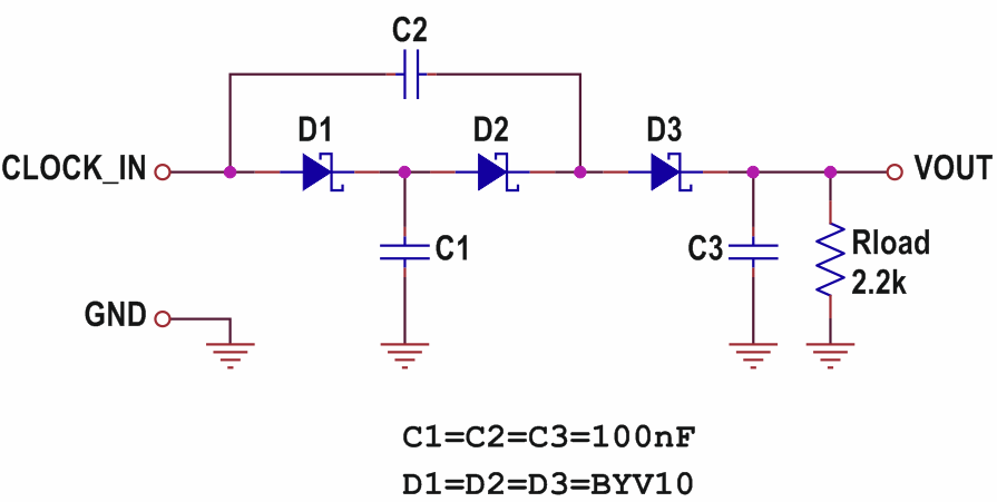
The voltage doubler described in this Design Idea is a modification of the Dickson charge pump. Unlike that circuit, it needs no DC input voltage, but only a digital clock whose peak value is ideally doubled at the output as a DC voltage.
The circuit acts as a charge pump, in which C1 charges to the high level of the input clock and then discharges through D2 into C2 on its low level. C2 in turn discharges into C3 through diode D3 when the clock returns high.
 |
|
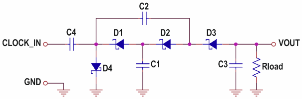
| Figure 1. | Voltage doubler generates its own local V+. |
With no load, the output voltage is twice the peak input voltage, minus the forward voltage of the three diodes – about 0.75 V total. The output voltage stabilizes within ten clock periods; after two clocks, it reaches about 60% of the final value. Its value depends on the load current and the peak value of the input clock, so if you want a precise output voltage you can always post-regulate.
To choose the value of the capacitors for your application you can use the following formula:
where ILOAD is the load current, TLOW is the duration of the clock’s low level, and VR (P-P) is the peak-to-peak ripple voltage acceptable at the output.
 |
|
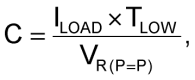
| Figure 2. | Added anti-ringing clamp D4. |
The circuit has been tested with a 200 kHz RC-Schmitt astable built with a 74HC14 inverter powered at VDD = 5 V (Figure 2). A 10 m twisted cable connected the output of the astable to the voltage doubler input, and the following measurements were obtained:
|
RLOAD
|
VOUT
|
VR (P-P)
|
|
No load
|
9 V
|
0 V
|
|
2.2 kΩ
|
8 V
|
120 mV
|
D4 minimizes ringing on the falling edge of the input clock.
The circuit, getting power from any digital data line, can be used to provide a higher supply voltage in remote micropower applications not using local batteries, such as in a 1-Wire serial interface network.
 |
|
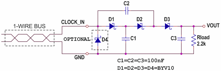
| Figure 3. | Voltage tripler. |
If you need an even higher supply voltage, you can expand the circuit to obtain an N-times multiplier. Figure 3 shows a 3-times multiplier.
 |
|
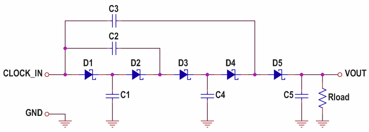
| Figure 4. | Negative voltage doubler. |
A negative voltage can also be created by inverting all the diodes and capacitively coupling and clamping the input peak to 0 V. Figure 4 shows a negative voltage doubler, with the clamping circuit comprising C4 and D4. You can also obtain higher negative voltages by modifying the Figure 3 circuit.