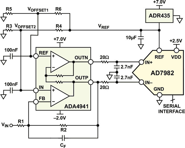
Circuit Function and Benefits
There are many applications that require a single-ended analog signal, either bipolar or unipolar, to be converted by a high resolution, differential input ADC. This dc-coupled circuit converts a single-ended input signal to a differential signal suitable for driving the AD7982, an 18-bit, 1 MSPS member of the PulSAR family of ADCs. This circuit uses the ADA4941-1 single-ended-to-differential driver and the ADR435 ultralow noise 5.0 V voltage reference. The circuit can accept many types of single-ended input signals, including bipolar or unipolar, ranging from high voltage to low voltage. Direct coupling is maintained throughout. If board space is at a premium, all the ICs shown in Figure 1 come in small packages, either 3 mm × 3 mm LFCSP or 3 mm × 5 mm MSOP.
 |
||
| Figure 1. | Single-Ended-to-Differential DC-Coupled Driver Circuit. (Simplified Schematic). | |
Circuit Description
The differential input voltage range of the AD7982 is set by the voltage on the REF pin. For VREF = 5 V, the differential input voltage range is ±VREF = ±5 V. The voltage gain (or attenuation) from the single-ended source, VIN, to OUTP of the ADA4941-1 is set by the ratio of R2 to R1. The ratio of R2 to R1 should be equal to the ratio of VREF to the peak-to-peak input voltage at VIN. For a peak-to-peak, single-ended input voltage of 10 V and VREF = 5 V, the ratio of R2 to R1 should be 0.5. The signal at OUTP is inverted (gain = –1) by the upper half of the ADA4941-1, which supplies the opposite phase output signal at OUTN. The absolute value of R1 determines the input impedance of the circuit. Feedback capacitor CF is chosen based on the desired signal bandwidth, which is approximately
The 20 Ω resistors and the 2.7 nF capacitors act as a 3 MHz single-pole low-pass noise filter.
Resistors R3 and R4 set the common-mode voltage on the IN– input of the AD7982. The value of this common-mode voltage is
where
Resistors R5 and R6 set the common-mode voltage on the IN+ input of the ADC. This voltage is equal to
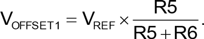
The ADC’s common-mode voltage, which is equal to VOFFSET1, should be close to VREF/2. This implies that R5 = R6. Table 1 shows some possible standard 1% values for the resistors for popular input voltage ranges.
| Table 1. | Circuit Values and Voltages for Popular Input Voltage Ranges | ||||||||||||||||||||||||||||||||||||
|
|||||||||||||||||||||||||||||||||||||
Note that the ADA4941-1 operates on supply voltages of +7 V and –2 V. Since each output must swing from 0 V to +5 V, the positive supply voltage should be a few hundred millivolts greater than +5 V and the negative supply should be a few hundred millivolts more negative than 0 V. For this circuit, supply voltages of +7 V and –2 V were chosen. The +7 V supply also provides sufficient headroom to power the ADR435. Other voltages are possible, provided the absolute maximum total supply voltage on the AD4941-1 does not exceed 12 V and the headroom requirement of the ADR435 is observed.
The AD7982 requires a +2.5 V supply for VDD as well as a VIO supply (not shown in Figure 1), which can range between 1.8 V and 5 V, depending upon the I/O logic interface levels. This circuit is not sensitive to power supply sequencing. The AD7982 inputs can withstand up to ±130 mA maximum during momentary overvoltage conditions.
The AD7982 SPI-compatible serial interface (not shown in Figure 1) features the ability, using the SDI input, to daisy-chain several ADCs on a single 3-wire bus and provides an optional busy indicator. It is compatible with 1.8 V, 2.5 V, 3 V, and 5 V logic, using the separate VIO supply. Excellent layout, grounding, and decoupling techniques must be utilized in order to achieve the desired performance from the circuits discussed in this note. As a minimum, a 4-layer PCB should be used with one ground plane layer, one power plane layer, and two signal layers.
All IC power pins must be decoupled to the ground plane with low inductance, multilayer ceramic capacitors (MLCC) of 0.01 μF to 0.1 μF (this is not shown in Figure 1 for simplicity). Follow the recommendations on the individual data sheets for the ICs referenced in the Learn More section.
Common Variations
For different reference voltages, the ADR43x family of references has a wide range of values that can interface with the ADC.
Learn More
Kester, Walt. 2005. The Data Conversion Handbook. Chapters 6 and 7. Analog Devices.
Kester, Walt. 2006. High Speed System Applications. Analog Devices. Chapter 2, “Optimizing Data Converter Interfaces.”
MT-031 Tutorial, Grounding Data Converters and Solving the Mystery of AGND and DGND. Analog Devices.
MT-035 Tutorial, Op Amp Inputs, Outputs, Single-Supply, and Rail-to-Rail Issues. Analog Devices.
MT-074 Tutorial, Differential Drivers for Precision ADCs. Analog Devices.
MT-101 Tutorial, Decoupling Techniques. Analog Devices.
Voltage Reference Wizard Design Tool.