[Editor’s note: This programmable DC reference & calibrator will make a great DIY project for your lab bench. Full design files for the analog portion are provided, leaving the microcontroller part up to you. Send me your code if you build this and I’ll append a download link to the article. Michael.dunn at aspencore.com]
This article describes a homemade DCV calibrator that offers a good balance between complexity, accuracy, and cost. Use it to check equipment, calibrate ADCs, and wherever you need an accurate voltage source.
Structure, parts, features
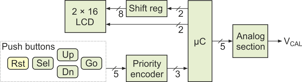
Figure 1 shows the block diagram of the calibrator. Five push buttons and a two-line display allow the user to set a voltage from –5 to +10 V with 100 µV resolution. The µC (microcontroller) also controls the analog section, which includes a high precision DAC (digital-to-analog converter), two analog switches, two op-amps, and four matched resistors. The whole circuit needs 12 I/O lines from the µC. The power supply is ±12 V.
 |
||
| Figure 1. | The calibrator has a simple user interface and requires only 12 I/O lines from the microcontroller in my implementation. More available I/O pins would allow further simplification. |
|
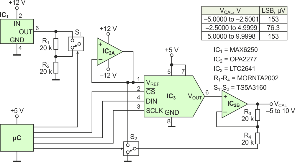
Figure 2 presents the analog section of the calibrator. The key part is the LTC2641, a 16-bit DAC from Linear Technology with differential and integral linearity of ±0.5 LSB each (typical). Offset and gain errors are 2 LSB max. and ±2 LSB typical, respectively.
 |
||
| Figure 2. | Three precision ICs, four matched resistors, and a microcontroller build a DC calibrator with 16-bit resolution and 70 µV error. |
|
The other parts in the circuit are of corresponding quality. The MAX6225 is a 5 V reference with 1 mV (200 ppm) tolerance and 2 ppm/°C drift. The OPA2277 is a dual high-precision op-amp with a maximum offset of 10 µV and drift of 0.1 µV/°C. The four 20 kΩ resistors are matched with ratio tolerance of 0.01% and temperature coefficient of 25 ppm/°C. The on-resistance of the analog switches is only 1 Ω; 0.005% of the value of the matched resistors (important for resistor R4).
S1 & S2 enable four ranges: 0-5 V, 0-10 V, ±2.5 V, and ±5 V, with resolution of 76.3 or 153 µV. The µC automatically selects the best range for the desired output.
Operation is simple and intuitive. The Reset (Rst) button resets the output voltage to 0.0000 V. The Select (Sel) button selects a character (sign or digit) on the display and makes it blink. The Up and Down (Dn) buttons modify the value of the blinking character. When the Go button is pressed, display stops blinking. Other control arrangements can of course be implemented.
The µC calculates a 16-bit number, sends it to the DAC, and controls the analog switches. Error messages are displayed when the desired voltage is less than –5.0000 V or greater than 9.9998 V.
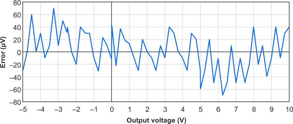
Circuit performance was tested with a 6.5-digit DMM from Keysight. As Figure 3 shows, the maximum error is ±70 µV, half of the 153 µV resolution of the circuit for the 10 V spans (0-10 V and ±5 V). For the 5 V spans, resolution drops in half and the error follows at ±40 µV max. These are the minimum possible values one can obtain with a 16-bit DAC and a 2.5 or 5 V reference. Errors fit well the 100 µV resolution of the display. Noise was under 1 µV.
 |
||
| Figure 3. | A 64-point calibration shows absolute error of ±40 µV for the 5 V spans and ±70 µV for the 10 V spans. |
|
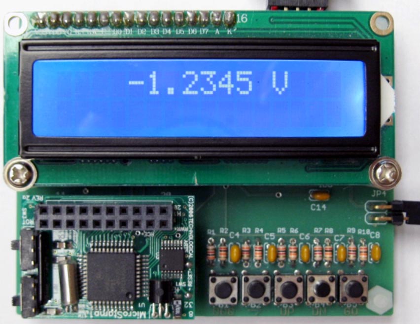
My version of the calibrator was built using a modular approach (Figure 4). The motherboard measures 82 × 67 mm. It carries most of the components and two connectors: a 16-pin connector for the display and a 20-pin connector for the µC board.
 |
||
| Figure 4. | My calibrator implementation uses a custom analog motherboard with µC and LCD plug-ins. |
|
Building and coding
The motherboard was designed with EAGLE (the design files include Gerbers). If you wish, you can replace the 20-pin connector with a connector that fits the board of your particular controller. You can also remove the connector and place your µC on the motherboard.
Once you have the board you have to design the firmware. The code has two major sections: initialization and a button-service loop.
The initialization stage does the following:
- Set up I/O ports of the micro
- Initialize display
- Put a welcome greeting on the display for few seconds
- Place the value of 0.0000 V on display
- Generate output voltage of 0.0000 V with the analog section
The button service is an endless loop. When a depressed button is found, the following actions take place:
The Reset button:
- Place the value of 0.0000 V on the display and generate output voltage of 0.0000 V
The Select button:
- When the button is pressed for the first time, the sign character on display starts blinking.
- If the Select button is pressed again, the next character will blink. If the last character is currently blinking, start over with the sign character.
When the Up button is pressed, reaction depends on what character is blinking:
- If the sign is blinking, reverse the sign
- If a digit is blinking, increase the value of that digit by one. If the current value is 9, the new value should be 0.
When the Down button is pressed, reaction depends on what character is blinking:
- If it is the sign, reverse the sign
- If it is a digit, decrease the value by one. If the current value is 0, the new value should be 9.
The Go button implements the following table.
The steps are:
- Ignoring sign and decimal point, convert display string into a number NLCD
- Based on the sign of the display string and the value of NLCD, define the range number presented in the second column of the table.
- When the range number is from 1 to 4:
- Calculate NDAC (the number to be sent to the DAC) using the formulas in the third column of the table.
- Send out NDAC to the DAC.
- Send out control signals to the switches as presented in the last two columns of the table.
- Return to the beginning of the button service loop.
- When the range number is 5 or 6, display error message and return to the beginning of the button service loop.
Write the code in your favorite language. C makes calculations easy and development relatively quick, though the generated code can be quite large. Assembly language goes the opposite way: small machine code and easy communication with the I/O devices, but harder calculations and longer development time.
The DAC is very linear, but offset and gain errors can be relatively large. To get the best performance from your calibrator, check it with a good DMM (6.5 digits or more). If errors are larger than 38 or 76 µV (depending on the range), adjust the numbers you send to the DAC.
For reference, I used a MicroStamp11 microcontroller from Technological Arts [1] and wrote the code in assembly language. The machine code requires 1550 bytes of EEPROM and 34 bytes of RAM. Due to the long numbers, multiplication and division are emulated with shift–add and shift–subtract instructions. Small offsets had to be included for three of the four ranges to minimize the error of the generated voltage. The SPI interface to the DAC is emulated using the general-purpose I/Os.