Marco Pisani
EDN
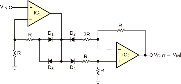
The circuit in Figure 1 delivers the absolute value of the input signal with an accuracy better than 10 ppm of the full-scale range. The circuit has low zero-crossing error. You can use it as an asynchronous demodulator, as a source for logarithmic amplifiers, or simply as a demonstration of the wonders of feedback. The circuit uses two op amps; five identical resistors, R; one double-value resistor, 2R; and thermally match diodes.
 |
||
| Figure 1. | This full-wave rectifier circuit yields the accurate absolute value of the input signal. | |
When the input, VIN, is positive, IC1's output is 2VIN + VD3 (the voltage drop across D3). D2 is reverse-biased, thus IC2 behaves as a voltage follower, yielding
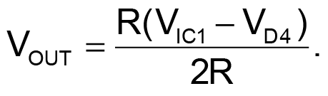
Because the same amount of current (VIN/R) flows in D3 and D4, assuming their characteristics are the same, VD3 = VD4, and VOUT = VIN. When VIN is negative, IC1's output is 2VIN - VD1. D4 is reverse-biased, and IC2 is an inverting amplifier, yielding
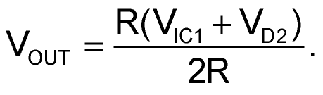
Again, the current flowing in D1 and D2 is VIN/R, and VOUT = -VIN. For good performance,
- The six resistors must match closely to guarantee symmetrical gain.
- The diode pairs, D1-D2 and D3-D4, must have tight thermal coupling to minimize errors at low input voltages. (It's best if the pairs are on the same chip.)
- The op amps must have low offset.
 |
||
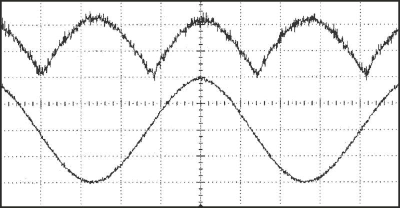
| Figure 2. | Even with a 40-mV p-p signal, the circuit in Figure 1 yields an accurate absolute value. |
|
In a practical configuration, you can configure D1 through D4 using base-collector junctions of a monolithic transistor array, such as an MPQ6700. The resistors are 10- and 20-kΩ, 1% metal-film units. You can use optional 100 Ω trimmers in series with the resistors in the circuit to trim for optimum performance. The op amps are OP27 devices, with their offset trimmed. After adjusting the op amps' offset and tweaking the resistors, the residual error is within 100 µV p-p over the 13 V p-p operating range. Figure 2 shows the behavior of the circuit with a 40-µV p-p input signal (bottom trace).