Unusual design constraints sometimes reveal the unfriendly side of everyday components and circuits. A case in point is the design of power-supply-regulation circuitry in which the primary power source has an absolute current-limit specification, such as spacecraft photovoltaic, or “solar,” panels and radioisotope-thermoelectric generators. Such applications require that you pay scrupulous attention to strict control of current consumption, including transient-current consumption, and infrequent consumption spikes, such as those that typically occur on power-up. The problem is that current-limited primary-power sources can suffer catastrophic voltage droop and shutdown in response to momentary overcurrent faults, even when the fault is brief. Common causes of such faults are the current spikes that charge the regulator output’s decoupling capacitor.
Unless the current limit of the regulator clips the resulting spikes, the spikes are equal to the regulator’s output-voltage rate of rise multiplied by the sum of the parallel output capacitances:
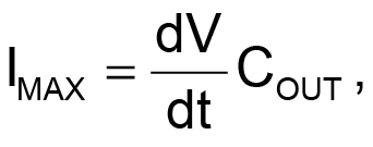
where IMAX is the maximum current, dV/dt is a differential in voltage with respect to a differential in time, and COUT is the output capacitance. The math suggests that the best strategy for limiting the regulator’s turn-on maximum current is to limit dV/dt. The circuit in Figure 1 relies on this trick and works with industry-standard adjustable linear regulators, such as the popular low-dropout LM2941.
 |
||
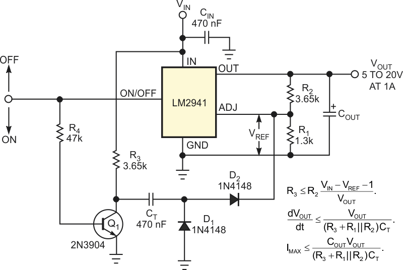
| Figure 1. | On power-up, the control current through R3, CT, and D2 delays the rise of VOUT and thus prevents excessive IMAX transients. |
|
The basis of the dV/dt-limiting technique comprises the six added components: R3, R4, CT, D1, D2, and Q1. On power-up, the control current through R3, CT, and D2 delays the rise of the output voltage and thus prevents excessive maximum-current transients.
Here’s how it works. When VIN is on and Q1 is off, current through R3, CT, and D2 pulls the adjust pin of the regulator to the reference. This action limits VOUT’s dV/dt to the rate of CT charging through the series resistance,
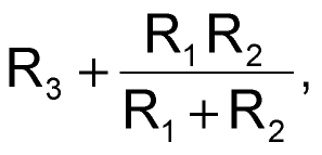
and thereby limits IMAX to any desired value using the design equations
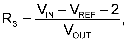
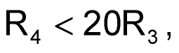
and
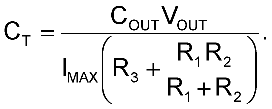
For example, given the circuit constants in the figure and assuming COUT = 100 µF, dV/dt = 2500 V/s, and IMAX = 0.25 A. At the end of the modified power-up sequence, D1 and D2 decouple the dV/dt circuit from the regulator’s feedback network, preventing the coupling of ripple voltages from the input voltage into the output voltage.