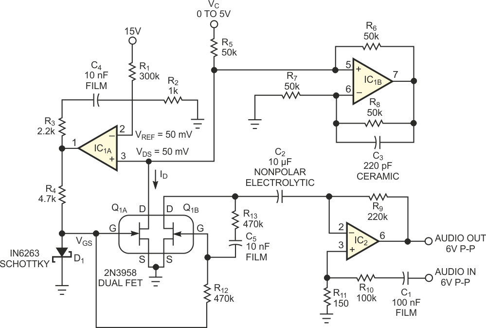
FETs find common use in VCAs (voltage-controlled amplifiers) and attenuators, in which the FET serves as a variable resistance. A control voltage applied to the gate sets the channel resistance and overall circuit gain. You frequently need to select individual FETs because of wide spreads in FET characteristics. The circuit in Figure 1 uses a master-slave servo technique with a matched-FET pair to implement voltage-controlled variable gain. This gain is a linear function of the applied control voltage, VC. In contrast with variable-gain circuits using a single FET as the gain-control element, the circuit in Figure 1 exhibits minimum gain for VC = 0 V and features a linear increase in gain with increasing VC. The self-biasing operation of the circuit also compensates for unit-to-unit variations in the FET characteristics, thereby making device selection less critical.
 |
||
| Figure 1. | This voltage-controlled amplifier has a dynamic range of –55 to 0 dB. | |
The circuit maintains the drain voltage, VDS, of Q1A at a low value (VREF = 50 mV) to ensure that the FET operates in the resistive region of its ID versus VDS characteristic curve. Op amp IC1A servos the VGS of Q1A to maintain VDS at VREF, while Q1A sinks the current from the Howland current source IC1B. The sourced current is
where VC is the control voltage. The channel resistance, RD, in kilohms is then
The same VGS applies to Q1B through R12. Because Q1 is a well-matched monolithic dual FET, Q1A and Q1B have identical channel resistance, RD. VGS varies from approximately 370 mV (which D1 limits to prevent gate-source conduction) to VP (approximately –1.7 V for the 2N3958) as VC varies from 0 to 5 V. IC2 is a variable-gain, noninverting amplifier, in which the controlled RD of Q1B sets the gain G:
The maximum gain is
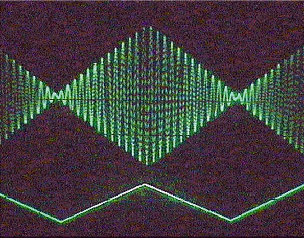
where R0 is the minimum channel resistance for VGS = 0 V, approximately 450 Ω for the 2N3958. The minimum gain is unity, when the FET does not conduct (VGS = VPINCHOFF). The circuit attenuates the audio-input signal level to lower than 10 mV p-p. This attenuation minimizes distortion in the FET and also sets the clipping level at the output of IC2. R13 and C5, in combination with R12, reduce distortion at higher signal levels. With the values shown, the gain increases linearly from –55 to 0 dB as VC varies from 0 to 5 V. The circuit accepts a 6 V p-p input signal. Figure 2 shows the result of modulating a 500-Hz sine wave with a 0 to 4 V triangle wave.
 |
||
| Figure 2. | A 0 to 4 V triangle wave linearly modulates the 500-Hz audio input. | |
For best performance, IC1 should be a low-offset, low-input-current unit, such as the OP290. IC2 should be a high-gain-bandwidth-product, low-noise amplifier, such as the NE5534. You can successfully use inexpensive units, such as the LF353 and LF351, at reduced gains. You can also operate the circuit from ±5 V supplies (with R1 changed to 100 kΩ), using an OP290 for IC1 and a TL031 for IC2. The maximum supply current for ±5 V operation is 0.33 mA, showing that low-power operation is possible.