Hua (Walker) Bai, Linear Technology
EDN
Internal operating voltages in electronic devices continue to decrease, but input-source voltages don't change. As the difference between input and output voltages increases, so does the improvement in efficiency that a switching regulator offers. Unfortunately, as a switched-mode step-down converter's output voltage decreases, the decrease imposes limitations on the circuit's input-voltage range. This Design Idea shows how to extend a low-output-voltage step-down converter's input-voltage range.
 |
||
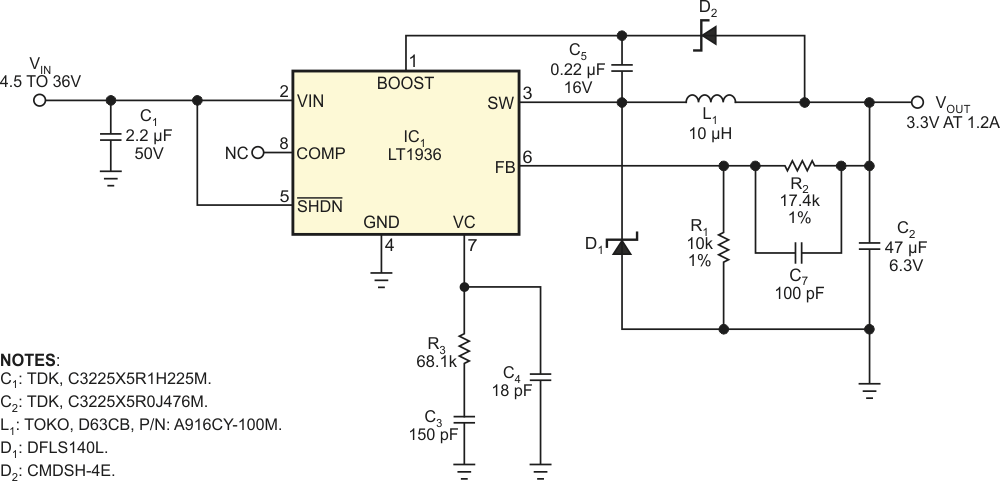
| Figure 1. | For efficient operation at output voltages of 3.3 V or higher, a charge pump comprising D2and C5 provides a voltage boost that provides sufficient drive for IC1’s internal switching transistor. |
|
A switching-mode step-down regulator, such as Linear Technology's LT1936 (IC1), includes an internal high-side NPN power transistor between its input, VIN, and switched-output (SW) pin. For highest efficiency, the high-side NPN transistor requires a base voltage that's higher than the input voltage. The circuit of Figure 1 works best for output voltages greater than 3 V. A charge pump comprising diode D2 and capacitor C5 maintains the voltage at the Boost pin 3 V above VIN. When IC1's internal power transistor switches off, the voltage at SW goes to ground through D1. Boost capacitor C5 charges to 3 V supplied from VOUT through D2. When the power transistor turns on, the voltage at SW jumps to VIN, and the voltage at the Boost pin jumps to VIN + 3 V, which provides sufficient head room to drive the power transistor into saturation for greatest efficiency.
 |
||
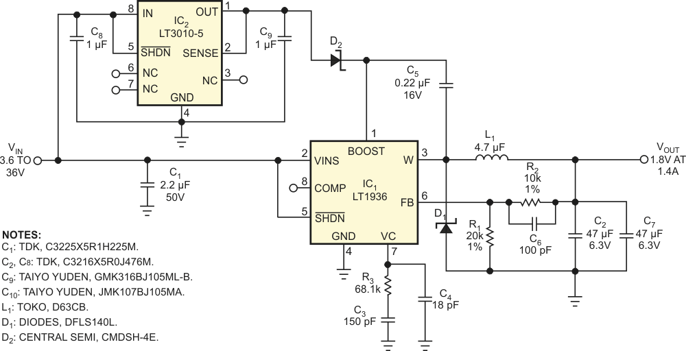
| Figure 2. | At outputs as low as 1.8 V, efficient operation at low input voltages benefits from an added low-dropout regulator, IC2, for the Boost pin, which extends the circuit’s input-voltage range. |
|
However, output voltages below 2.8 V no longer provide sufficient drive voltage to fully saturate IC1's switching transistor, and the circuit's efficiency suffers due to increased voltage drop across the transistor. In this situation, connecting D2's anode to VIN instead of VOUT doubles the Boost pin's voltage to twice the value of VIN but limits VIN to 20 V to avoid exceeding the Boost pin's allowable maximum voltage. For outputs lower than 2.8 V, the circuit in Figure 2 extends VIN's maximum voltage to 36 V. When the input exceeds 5.3 V, a Linear Technology LT3010-5 low-dropout voltage regulator maintains the voltage across C9 at 5 V. As a result, for input voltages at VIN of 5.3 to 36 V, the voltage at the Boost pin always remains at 5 V above VIN.
 |
||
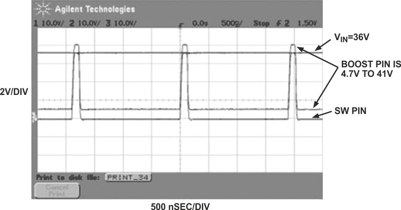
| Figure 3. | At a maximum input voltage of 36 V (VIN), waveforms at the SW and Boost pins show a 5 V boost-voltage margin for the circuit of Figure 2. |
|
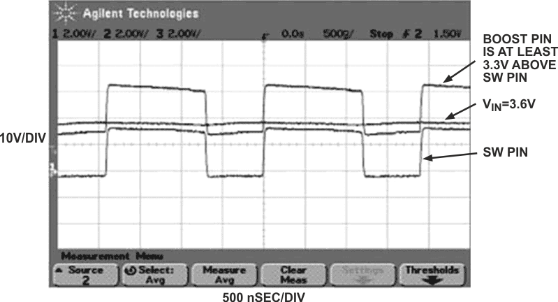
Figure 3 shows a 36 V input applied to VIN and the resultant voltages at the SW and Boost pins. In Figure 3, the maximum Boost-pin voltage reaches 41 V, safely below the pin's 43 V maximum rating. For values of VIN of 3.6 to 5.3 V, IC2 operates in dropout mode and introduces only a 300-mV drop from its input to its output. Figure 4 shows that, even at the circuit's minimum 3.6 V input, the Boost pin remains 3.3 V above VIN, and IC1's internal NPN transistor receives sufficient drive voltage for saturated operation.
 |
||
| Figure 4. | At 3.6 V input (VIN) and 1.8 V output, a voltage of 3.3 V at IC1’s boost pin ensures that IC1’s internal switch still operates in saturated mode. |
|