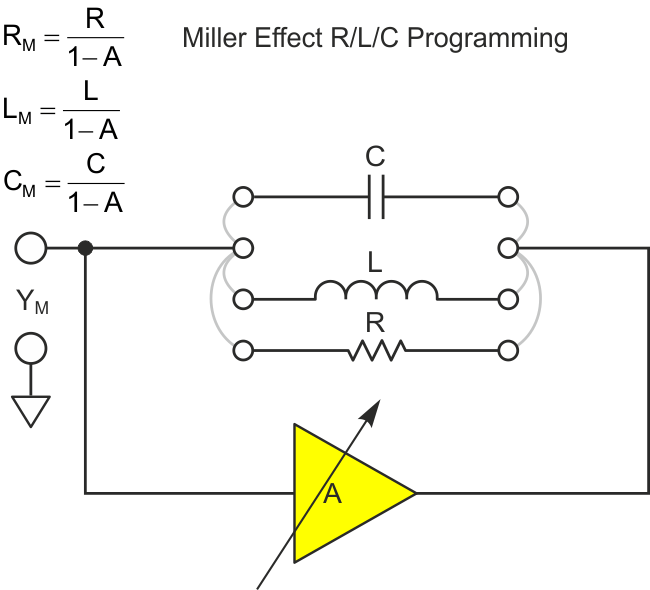
The Miller effect, first reported a century ago, causes impedances connected between input and output of a voltage amplifier to be reflected in the amplifier input impedance, proportionately scaled by amplifier gain. Although first seen as only an undesired parasitic-capacitance multiplier limiting bandwidth and stability, the Miller effect has also been incorporated into useful topologies, like analog oscilloscope timebase integrators.
 |
||
| Figure 1. | Variable-gain Miller effect scaling of feedback impedance. | |
This Design Idea suggests another cool way to use it, based on the fact that if amplifier gain (A) is made variable, then the reflected Miller impedance (ZM) or susceptance (YM) will be too (Figure 1).
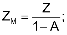
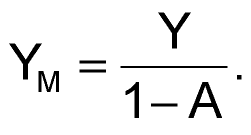
Note in particular the interesting effect of allowing the range of gain factor A to include A = +1 and thus (1 – A) = (1 – 1) = 0, which causes ZM (i.e., LM or RM) to go (theoretically) to infinity and YM (CM) to zero.
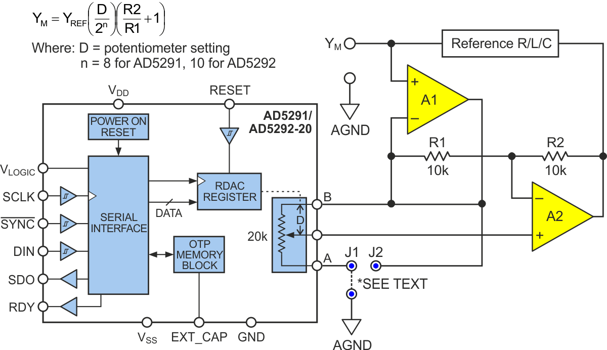
A practical realization of the Miller effect component synthesis circuit is suggested in Figure 2.
 |
||
| Figure 2. | Example variable-gain Miller circuitry. | |
Selection of the gain-setting potentiometer (simple analog trimmer, precision pot with turns-counting dial, or the illustrated digital pot) reflects application requirements. Selection of A1 and A2 accommodates needed bandwidth, voltage compliance, and current drive capability, while the R2/R1 ratio determines gain adjustment range: (+1 to –R2/R1). For example, given the components shown (e.g., 10-bit resolution AD5292-20 digital pot), R1 = R2, YREF = 0.5 µF reference capacitor, and jumper J1 connected to ground, YM can be synthesized from ~zero (single digit pF) to 1.0 µF in 1k steps of ~1 nF (actually 977 pF):
The resulting circuit is useful in prototyping, testing, post-production trimming, tuning, and calibration.
However, the reader will have noticed an obvious limitation. The synthesized reactance has only one active terminal, with the other implicitly grounded. This is problematic in many potential applications, but when access to both terminals is required, a solution exists (Figure 3).
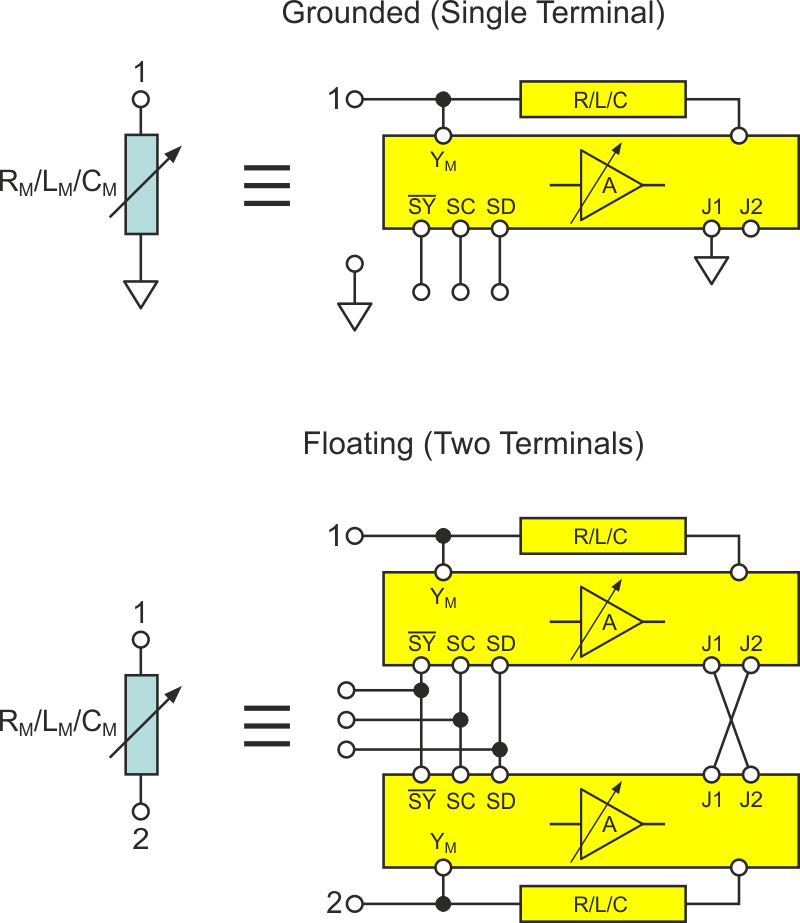 |
||
| Figure 3. | One- and two-terminal topologies. | |
It takes advantage of the differential signal appearing across the synthesized reactance with a J1/J2 cross-connection between two identical Miller circuits (both incorporating the same reference reactance and pot setting), one for each terminal. In this way, the Miller gain amplifiers in both circuits subtract the signal appearing at the opposite terminal, effectively synthesizing a floating component between the terminals.