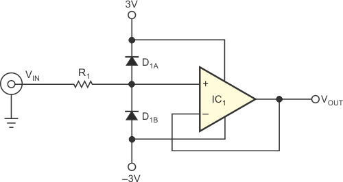
Certain measurement applications, such as for pH (acidity) and bio-potentials, require a high-impedance buffer amplifier. Although several semiconductor manufacturers offer amplifier ICs featuring low bias and offset-input currents, attaching a sensor cable to an amplifier circuit can inflict damage from ESD (electrostatic discharge). Figure 1 shows one unsatisfactory approach to ESD protection. Resistor R1 limits an ESD event's discharge current, and diodes D1A and D1B clamp amplifier IC1's input to its power-supply rails. Unfortunately, when shunting a pH sensor's 400-MΩ input impedance, even low-leakage diodes, such as ON Semiconductor's MMBD1503A, introduce significant offset voltages.
 |
||
| Figure 1. | In a conventional ESD-suppression circuit, diodes clamp an amplifier’s input voltage to its power-supply rails but introduce unwanted leakage currents. |
|
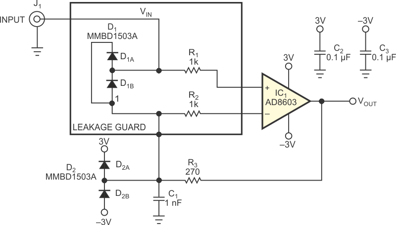
The circuit in Figure 2 offers an alternative approach. An Analog Devices low-input-bias, low-offset-current AD8603 amplifier, IC1, serves as a unity-gain input buffer. For any normal input, the circuit's output voltage, VOUT, equals its input voltage, VIN. Thus, the voltage across ESD-protection diode D1A or D1B approaches 0 V, and neither diode's leakage current affects the sensor's output signal. Depending on the polarity of an ESD event you apply to the circuit's input connector, its high-voltage spike discharges through diode D1A or D1B into the positive or the negative power-supply rail. Capacitor C1 acts as an intermediate "charge reservoir" that slows the ESD spike's rate of rise and protects IC1's output stage from latching until diode D2A or D2B begins diversion of the ESD transient into the positive or the negative supply rail. In effect, C1 compensates for D1's parasitic capacitance. Resistor R3 allows IC1 to drive the capacitive load that C1 presents without going into oscillation.
 |
||
| Figure 2. | In this alternative design, voltage across both halves of D1 normally approaches 0 V and introduces no leakage currents. During an ESD event, both D1 and D2 conduct to protect IC1’s inputs. |
|
During an ESD event, both D1 and D2 can conduct, but the voltage at VIN exceeds the power-supply-rail voltage by only two forward-biased diode voltage drops. Resistors R1 and R2 limit the amplifier input's currents below the manufacturer's recommended 5-mA maximum rating.
 |
||
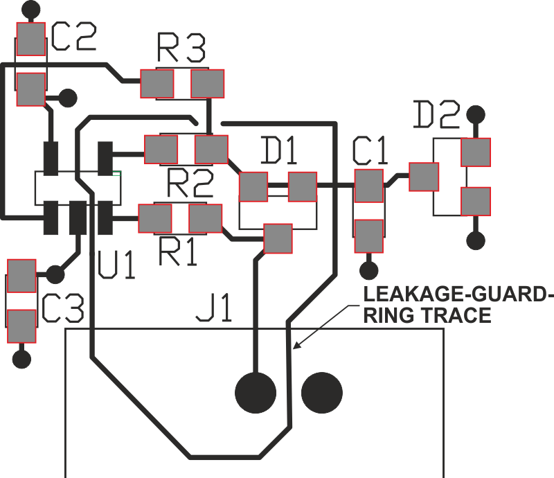
| Figure 3. | For best performance, place copper traces around the amplifier’s high-impedance points to intercept leakage currents. |
|
When packaging the circuit, pay special attention to the pc board's layout. Imperfections in the board's dielectric properties can provide parasitic-leakage-current paths. Adding copper traces on both sides of the board to form guard rings around the circuit's high-impedance nodes diverts leakage currents (Figure 3).