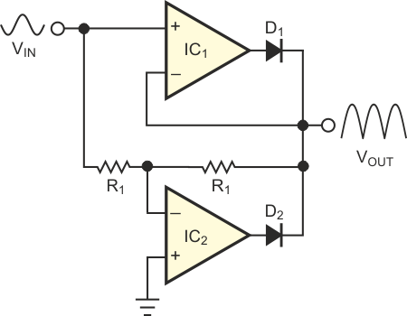
The traditional approach to the design of a full-wave rectifier (Figure 1) is to set the gains of IC1 and IC2 to 1 and use the steering diodes D1 and D2 to sum the sinusoidal half-cycles of the input to form the rectified output. For the positive half-cycle of the input signal, IC1 is a noninverting amplifier with a gain of 1. For the negative half-cycle of the input signal, IC2 is an inverting amplifier with a gain of –1.
 |
||
| Figure 1. | This full-wave-rectifier circuit has a fixed gain of 1. | |
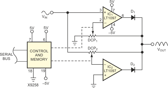
This full-wave-rectifier circuit often combines with a lowpass filter to form a low-cost ac/dc converter. If you need a full-wave rectifier with amplification, the combination of these two functions in one circuit can provide savings in cost, component count, and board space.
 |
||
| Figure 2. | You can program the gain of this full-wave rectifier from unity to 255. | |
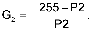
The circuit in Figure 2 combines rectification and programmable amplification. The two 256-tap digitally controlled potentiometers, DCP1 and DCP2, control the gains of the noninverting amplifer, IC1, and the inverting amplifier, IC2, respectively. The gain of IC1 is
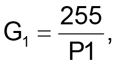
where P1 (0≤P1≤255) is the programmed decimal value of DCP1. Similarly, the gain of IC2 is
The performance of this circuit takes advantage of the resistor matching inherent in the digital potentiometers. The measured data falls within 2% of calculated values.