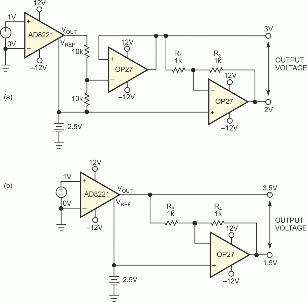
State-of-the-art ADCs accept differential inputs, allowing you to differentially implement the entire signal path from sensor to converter. This structure provides significant performance advantages, because differential signals increase the dynamic range, reduce hum, and eliminate ground noise. Figures 1a and 1b show two common differential-output instrumentation-amplifier circuits. The first provides unity gain, and the second implements a gain of two. Both circuits, however, suffer from increased noise, offset error, offset drift, gain error, and gain drift as compared with an instrumentation amplifier with a single-ended output.
 |
||
| Figure 1. | The differential-output circuits having unity gain (a) and a gain of two (b) suffer from high noise level, excessive offset error and drift, and significant gain error and drift. |
|
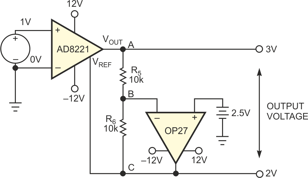
Figure 2 shows a differential-output instrumentation amplifier that has none of these deficiencies. The design exploits the fact that the output of an instrumentation amplifier is the difference between the output pin, VOUT, and the reference pin, VREF. This application adds an inverter with a gain of –1 between the two pins.
 |
||
| Figure 2. | This differential-output instrumentation amplifier preserves the gain and adds no offset, drift, or noise to the output signal. |
|
With an input voltage, V, the output voltage (VOUT–VREF) must also be equal to V. The reference pin's voltage is opposite in polarity to the output pin's voltage. Therefore, the output must produce
and
to satisfy
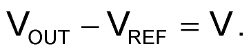
 |
||
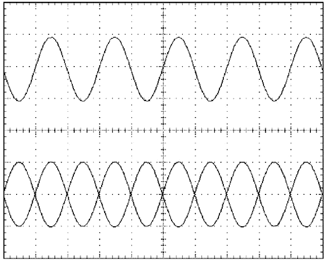
| Figure 3. | A 2 V p-p, 1-kHz input signal (top), and 1 V p-p differential-output signals (bottom) have an output common-mode voltage of 2.5 V. |
|
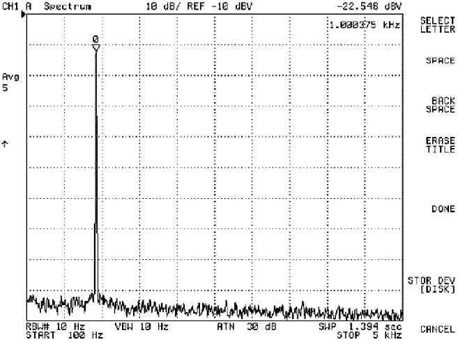
Applying a 2.5 V signal to the noninverting terminal of the op amp sets the common-mode output level. The op amp establishes 2.5 V at Node B. Accordingly, if you apply 1 V to the input, 3 V appears at Node A, and 2 V appears at Node C. Thus, the output is 0.5 V higher than and 0.5 V lower than 2.5 V. Errors from VOUT – VREF are a function only of the instrumentation amplifier. Errors such as offset, noise, and gain error that stem from the inverter amplifier and resistors equally affect both outputs. Thus, they contribute only to the common-mode output, which the ADC rejects. The top waveform in a performance photo shows the 2 V p-p, 1-kHz input (Figure 3). The two outputs appear at the bottom. The output common-mode voltage is 2.5 V. Another performance photo shows the spectral density of the differential output (Figure 4).
 |
||
| Figure 4. | The spectral analysis of the differential-output signal shows that input to the instrumentation amplifier is 2 V p-p, 1 kHz. |
|