The circuit in Figure 1 is an alternative to a high-side current monitor in a recent Design Idea (Reference 1). That monitor uses the Analog Devices AD8212 and an external high-voltage bipolar PNP transistor. The AD8212 can compensate for errors, which can reduce from the approximately –1% error of an uncompensated circuit to about –0.4%.
 |
||
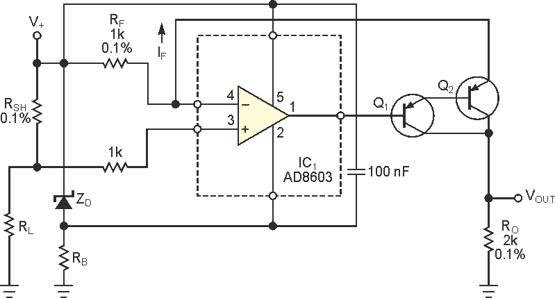
| Figure 1. | The circuit senses the current flowing through load resistor RL at the high side and transfers it directly to the low side by means of feedback current IF, which has 500 μA at full-scale. |
|
Circuit errors occur mainly because of the finite current gains of the two bipolar PNP transistors in the circuit: an external transistor and an internal low-voltage PNP transistor in the AD8212. The internal PNP transistor’s base-emitter junction forms a negative-feedback loop for the op amp within the AD8212. Both PNP transistors form a cascade of two common-base-operated transistors. In the ideal case, the emitter current of the internal PNP, which is proportional to a sensed current, should equal the collector current of the external PNP. This collector current mediates the information about the sensed current. In practice, however, the collector current of the external PNP transistor equals the emitter current of the internal PNP minus the sum of the base currents of both PNP transistors.
The base current is also a source of error in this circuit. The circuit reduces the undesired base current of the Darlington PNP by a factor of one divided by βPNP compared with the circuit in the earlier Design Idea. In that Design Idea, βPNP is the current gain of one PNP transistor. The circuit in Figure 1 reduces error by using a PNP-to-Darlington connection in place of an external PNP transistor. The difference between the emitter and the collector currents in the Darlington connection is so low that you can omit compensation circuitry and the internal PNP transistor, which are associated with the compensation circuit. You could thus integrate the two 1-kΩ resistors and the zener diode into a monolithic IC that is simpler than the AD8212.
The circuit in Figure 1 uses an Analog Devices AD8603 op amp, which has a 40-µV input offset voltage. When its input voltage is close to the upper supply rail, the offset voltage is less than 200 µV. The worst-case input offset-voltage value would cause an additive error of 0.04% of the full-scale because the full-scale is 500 mV. IC1’s subpicoampere input bias current rises at elevated temperatures to about 320 pA at 125 °C, but that increase is still not significant enough to affect circuit accuracy. The same holds true also for the leakage current of the Darlington connection because the leakage currents flowing through the emitter and the collector of Q2 have almost the same value. Leakage current ICE0 becomes a part of the feedback current that flows through resistor RF.
When ICE0 rises, the op amp’s output voltage goes slightly more positive. Feedback current IF, flowing through resistor RF, still remains constant. The only condition is that the minimum feedback current must be larger than the maximum leakage current. The selected PNP transistors allow V+ to be as high as 30 V. Q1, an MMBT3906 type, exhibits a low drop in the value of current gain at low emitter currents. It drops to just 75% of its maximum value of 130 at an emitter current of –100 μA. Q2 is an MMBT4403 type.
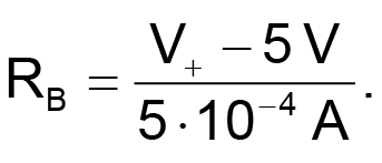
For applications requiring higher values of V+, select PNP transistors having sufficient collector-emitter voltage ratings and increase the value of RB as
ZD, a ZPY5V6, has a zener voltage of about 4.7 V at about 500 μA. A test reveals that the relative difference between the emitter and the collector currents of the Darlington pair doesn’t exceed 0.06% at full-scale. At 0.01 times full-scale, the relative error rises to 1.77%, indicating that the overall current-gain value of the Darlington decreases to about 56. The reduction of error lets you reduce the full-scale voltage at shunt resistor RSH to 250 mV, reduce the power dissipated in RSH by 50%, and maintain the error at 0.15%.