Inductors designed with active elements are very desirable to designers today because conventional spiral inductors are too big, too heavy, and too costly, and they require tuning. During the last few decades, various grounded inductors have been created using different high-performance active building blocks, such as operational amplifiers and operational transconductance amplifiers. But op amps suffer from a finite gain-bandwidth product (GBP) and GBP interdependence, so they can’t be used at high frequencies.
One alternative, a current-feedback operational amplifier (CFOA), is very popular because it overcomes the drawbacks of op amps. The design described here uses a commercially available CFOA, the AD844AN by Analog Devices, in a new synthetic, grounded lossy inductor. The inductor doesn’t use any external capacitors. Instead, internal capacitance appearing at the compensating pin of the CFOA is used, so the circuit could be classified as an active-R circuit.
 |
||
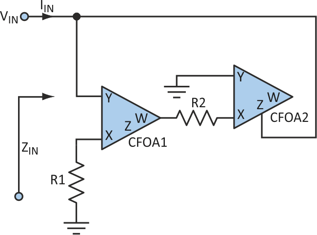
| Figure 1. | Just two current-feedback op amps and two resistors are needed to create a synthetic inductor that eliminates the drawbacks of other active-element inductors. |
|
A CFOA is an active building block and an ideal CFOA is characterized by the equations (see the Figure 1):
IY = 0
VY = VX
IZ = IX
VW = VX
Although the two CFOAs and the two resistors in the figure create a grounded inductor, this idea could be extended to create a floating inductor by using back-to-back connections.
Since no external resistor is present at terminal Z of CFOA1, the parasitic resistance must be considered for accurate analysis of the circuit. If the parasitic resistance and capacitance at terminal Z of the first CFOA are RO1 and CO1, and the parasitic resistance and capacitance at terminal Z of the second CFOA are RO2 and CO2, the input admittance is:
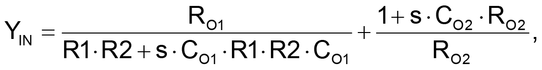
where s refers to the Laplace transform.
Note that RO is generally on the order of megohms and CO is generally in picofarads. With this in mind and assuming that R1 × R2 << RO1 and the frequency range for this design can’t exceed the megahertz range, the input impedance of the circuit is approximately:
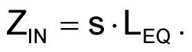
where
LEQ = C × R1 × R2.
The circuit was designed with R1 = R2 = 500 Ω (5% resistor value discrete). Using the AD844 datasheet and the experimental setups it provides, C = CO1 = 4.5 pF and RO1 = RO2 = 3 MΩ. Very low values of inductances were synthesized with tolerable differences between the theoretical and synthesized values. Typical values were of the order of microhenries. Such small inductor values are particularly suitable for RF designs.
The design presented here is simple, and the structure is well known. In addition, the readily available commercial CFOA ICs make the circuit very feasible and easy to implement.
References:
- K. Pal, “Floating inductance and FDNR using positive polarity current conveyors,” Active and Passive Electronic Components, Vol. 27, pp. 81-83, 2004.
- Raj Senani and V.K. Singh, “Novel Single-Resistance Controlled- Oscillator Configuration using Current Feedback Amplifiers,” IEEE Transactions on Circuits and Systems-I: Fundamental Theory and Applications, Vol. 43, No. 8, pp. 698-700,1996.