Tom Gay
EDN
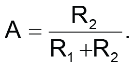
In low-power, single-supply analog applications, it is often desirable to maintain precise control of voltages much greater than the positive-supply rail. The circuit in Figure 1 allows you to amplify the input voltage, VIN, by a factor, A, which resistors R1 and R2 set. The output voltage, VOUT, equals AVIN, where
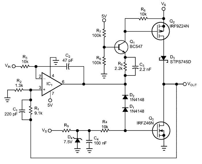
The op amp receives its supply from a single 5 V source, and the discrete output stage operates from a rectified voltage, VS, from a power source that meets the requirements of the application. When the circuit neither sinks nor sources current, the op amp’s output settles to a voltage higher than 1.9 V (Q1 is completely off) but lower than the threshold voltage of the n-channel FET, Q3, minus 1.2 V (two diode drops). When VIN rises from a given state, the op amp’s output voltage drops and gradually turns on Q1. This action results in a voltage drop across R8, turning on Q2. This process continues until the voltages at the op amp’s two inputs match. A decreasing VIN causes the op amp’s output voltage to rise to the point at which Q3 conducts enough to pull down VOUT. Capacitors C1, C2, and C3 are necessary to prevent oscillation.
 |
||
| Figure 1. | This simple circuit allows you to control voltages far in excess of the positive-supply rail. | |
The circuit, useful as a power driver for pulse generators, offers rise and fall times of less than 15 µsec, virtually independently of the supply voltage, VS. You can test the design with op amps LMC7101, LT1013, and AD8551. All these op amps deliver load currents as high as 5 A at voltages as high as VS = 40 V. One important feature of the design is its insensitivity to component tolerances. The values for R1 and R2 in Figure 1 yield A = 8. The value of R9 depends on VS. You could use a logic- level FET, such as the IRLZ34N for Q3; you can then omit the components D1, D2, D4, R4, R9, and C4. In this case, the op amp’s output connects directly to the gate of Q3, and you must reduce the value of R6 to lower the base voltage of Q1 to maintain the “idle window” in which both Q1 and Q3 are off. The op amp’s input-voltage range must include ground. D3 is necessary only in cases in which sources connect to the output. D3 prevents reverse current flow from the external source through Q2. Such a situation can arise when the circuit serves in a battery-charger application.