A high-resolution SAR ADC often needs a higher-order antialiasing filter, such as the third-order version provided by this low-noise, low-power design.
For many analog-to-digital converter (ADC) applications, a simple passive resistor/capacitor (RC) filter at the buffer input will provide adequate antialiasing filtering. However, an active filter is often needed for higher-resolution, low-noise applications that require higher-order filtering. The active component in that filter must have sufficient bandwidth, fast settling time, low noise, and low offset voltage so that it doesn’t corrupt the signal before it gets to the ADC.
 |
||
| Figure 1. | The 30-kHz, third-order active filter centered on op amp U2 drives the 24-bit ADC with the necessary bandwidth, fast settling time, low noise level, and low offset voltage. |
|
This circuit uses a differential op amp optimized to drive a low-power successive-approximation-register (SAR) ADC, although it will work for other converters as well (Fig. 1). It provides a 30-kHz, third-order filter based on op amp U2 (LTC6363), which has 500-MHz gain-bandwidth product, 780-ns settling time to 4-ppm, 2.9-nV/√Hz input-referred noise, and a maximum offset voltage of 100 µV. U2 is optimized to drive U1 (LTC2380-24), a 1.5/2-Msample/s, low-power SAR ADC with an integrated digital filter that can average from 1 to 65,536 conversion results in real time, thus providing an increase in signal-to-noise ratio (SNR).
 |
||
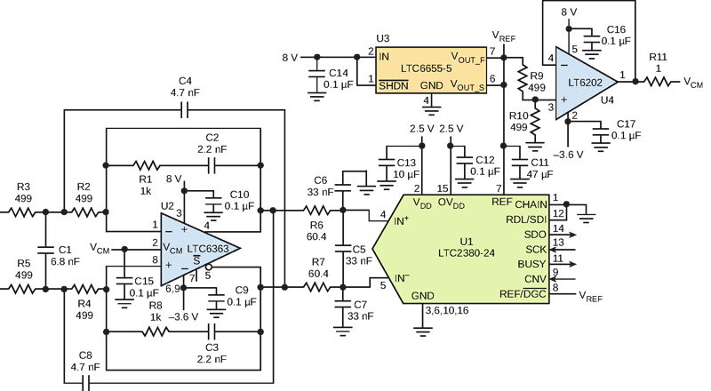
| Figure 2. | The combined frequency response of filter plus ADC is flat out to a 10-kHz input. |
|
The inputs of this circuit are driven differentially with a ±2.5-V p-p signal range via R3 and R5 (or one input can be grounded while the other input is driven with a signal that can range up to ±5 V p-p). The output of ultra-low-noise op amp U4 (LT6202) is applied to U2’s common-mode voltage input to establish its output common-mode reference voltage.
 |
||
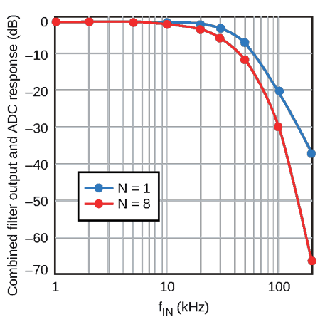
| Figure 3. | The PScope screen capture shows key parameters FFT, SNR, and THD of the circuit with N = 1. | |
High-quality capacitors and resistors should be used in the RC filter network between U2 and U1 (C5, C6, C7, R6, and R7), since these components can add distortion. NP0 and silver-mica type dielectric capacitors have excellent linearity, and metal-film surface-mount resistors are much less susceptible than carbon surface-mount resistors to generating distortion, which can result from self-heating, as well as damage that may occur during soldering.
 |
||
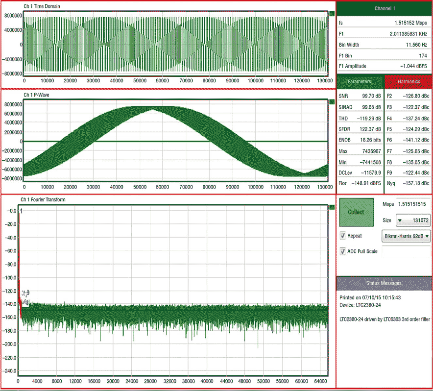
| Figure 4. | Details of THD versus input frequency show that it’s always below –60 dB, even at 100-kHz input frequency, for both N = 1 and N = 8. |
|
Figure 2 shows the combined frequency response of the filter and ADC with a sample rate of 1.5 Msamples/s and number of averages (N) set to 1 and 8. Figure 3 is a PScope screen capture that shows the fast Fourier transform (FFT), SNR, and total harmonic distortion (THD) for the circuit with N = 1. (PScope is a USB-based product demonstration and data-acquisition system for use with Linear Technology’s high-performance ADCs and signal-chain receiver family.)
 |
||
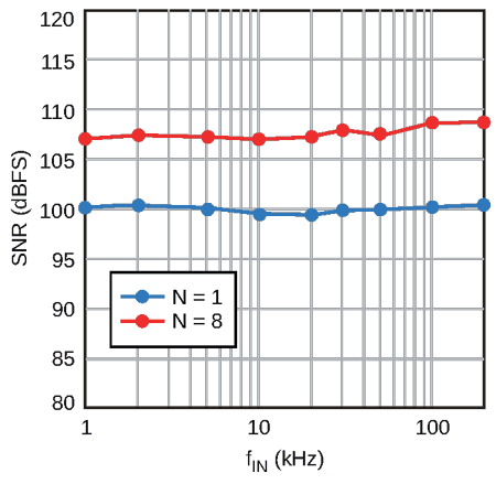
| Figure 5. | SNR is 100 dB and better out to 100-kHz input frequency, again for N = 1 and N = 8. |
|
Figures 4 and 5 respectively show THD and SNR versus input frequency, with N equal to 1 and 8. At input frequencies below a few kilohertz, performance is close to the typical datasheet numbers for SNR and THD, and THD gracefully degrades as the input frequency increases beyond that range.