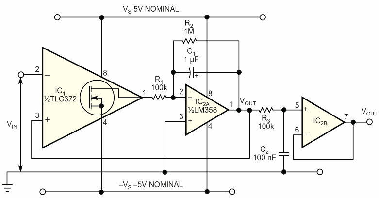
Requiring no rectifier diodes, the positive peak-detector circuits in figures 1 and 4 exploit the open-drain output of a Texas Instruments TLC372 fast comparator, IC1. Both versions of the detector are simple and inexpensive and provide a buffered, low-impedance output at VOUT. In addition, the TLC372's high typical input impedance of 1012 Ω eliminates any need for an input buffer stage. As Figure 1 shows, the detector's output voltage at the output of op amp IC2A applies a feedback signal for the comparator and acts as a reference level for comparison with the input signal's amplitude. Upon first application of input signal VIN, the voltage on the hold capacitor, C1, is 0 V, and VOUT is also 0 V.
 |
||
| Figure 1. | The dual-power-supply-voltage version of this positive peak detector requires only two active devices: a comparator and a dual operational amplifier. |
|
When the input signal goes more positive than the output voltage, the comparator's internal output MOSFET turns on and sinks current through. Provided that R2 is relatively large, charging current flows into C1 from IC2A's output. Over several cycles of the input signal, the charge on C1 builds up, and VOUT rises to the point at which it slightly exceeds the peak level of VIN. For as long as VOUT is slightly greater than VIN, IC1's output MOSFET remains off, and C1 receives no additional packets of charge.
As a consequence, the charge stored on C1 starts to dissipate as the capacitor discharges through R2 and through the bias-current path into IC2A's inverting input. VOUT gradually falls until it is just below the peak level of VIN. The next positive peak of VIN trips comparator IC1, which pulls current through R1, "topping up" the charge on C1. This process produces a dc level at VOUT that closely approximates the positive peak level of the input waveform. The values of R1, R2, and C1 determine the ripple voltage present on VOUT.
IC2A's inverting input is held at virtual ground potential, so whenever IC1's output MOSFET turns on, the voltage across R1 approximately equals the negative-supply-rail voltage, –VS. Therefore, using a small value of R1 injects a relatively large pulse of current into C1, thus allowing the circuit to respond quickly to a sudden increase in input-signal amplitude – that is, a "fast-attack" response. However, if the value of R1 is too small, the positive-going ripple on VOUT becomes excessive and can lead to bursts of oscillation around peak values of VIN.
For a given value of R2, the value of C1 determines the circuit's "delay time." A relatively large value of capacitance minimizes the negative-going ripple on VOUT, which can be useful when dealing with low frequencies, low-duty-cycle pulse trains, or both. However, making C1 too large renders the detector sluggish when responding to a sudden decrease in input-signal amplitude. Note that C1 also affects the attack time; for example, doubling the capacitance doubles the time the circuit takes to acquire the peak level of VIN.
 |
||
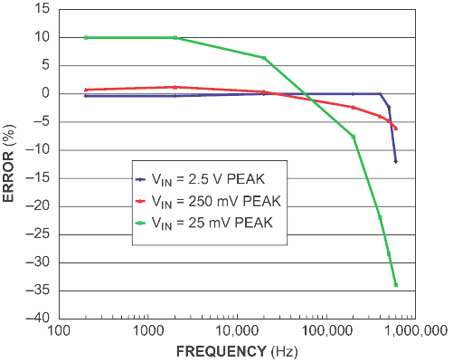
| Figure 2. | Plotting the difference between peak signal levels and output voltage for three peak levels illustrates the detector’s frequency response. |
|
Because the comparator's feedback path includes op amp IC2A, offsets and errors that IC2A presents have no effect on the circuit's accuracy. At low to moderate frequencies, only the comparator's input offset errors contribute to the detector's overall accuracy. At high frequencies, the comparator's response time becomes a significant factor, leading to a reduction in VOUT that worsens as the frequency increases. Despite these limitations, the circuit performs well over several decades of frequency from approximately 50 Hz to 500 kHz. Figure 2 and Table 1 show the test circuit's sine-wave-frequency response by plotting the error in VOUT for three peak levels of VIN.
| Table 1. | Sine-wave-frequency response | |||||||||||||||||||||||||||||||||||
|
||||||||||||||||||||||||||||||||||||
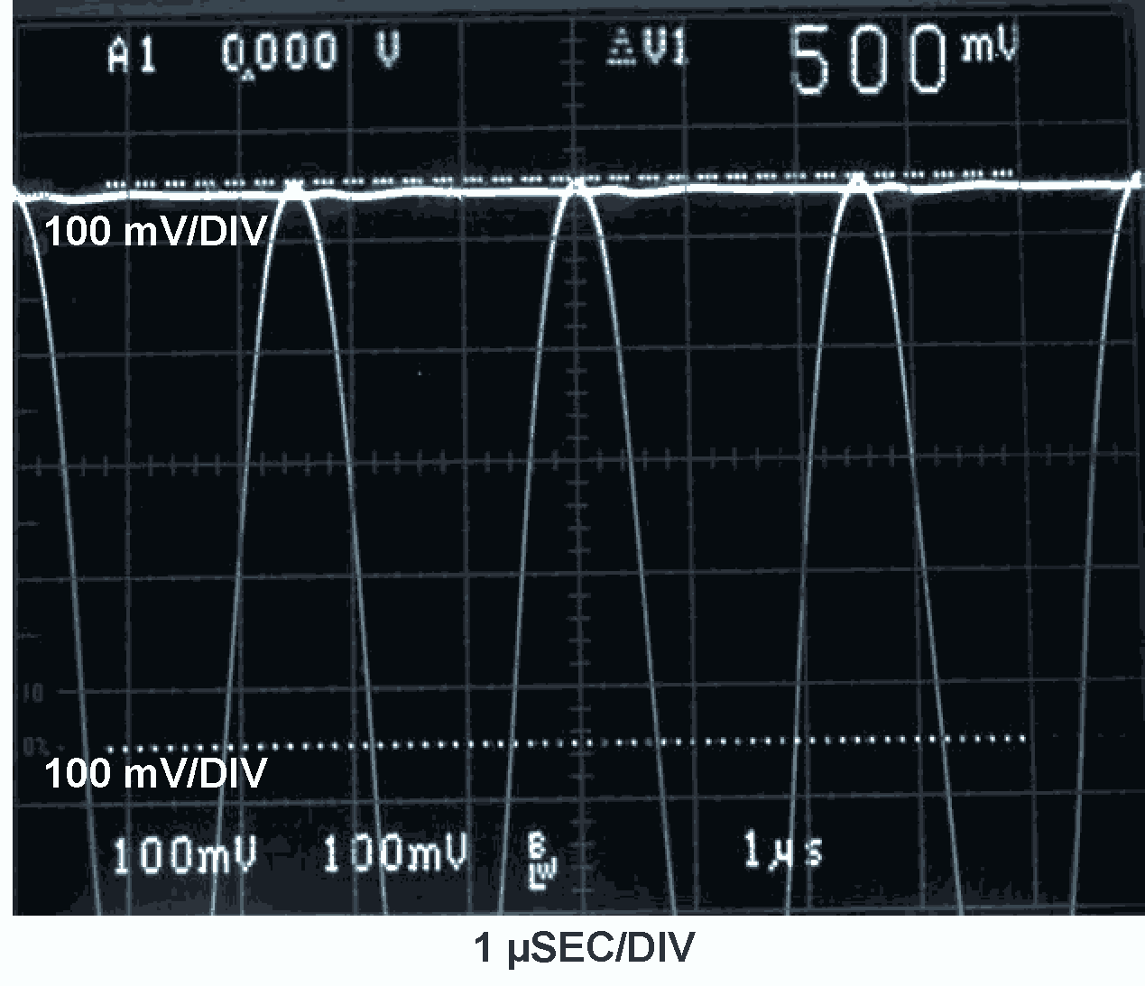
The oscilloscope photo shows the circuit's response to a 500-mV peak sine wave at 400 kHz, in which the output voltage, at 488 mV, lies just below the positive peaks (Figure 3). In addition to exhibiting good sine-wave response, the test circuit produces good results with rectangular signals of duty cycles as low as 5%. Note that the virtual ground at IC2A's inverting input restricts VOUT to positive voltages only. Therefore, the circuit can respond only to true positive peaks – that is, peaks that go above 0 V. If the input signal goes entirely below 0 V, VOUT simply levels off at 0 V.
 |
||
| Figure 3. | An oscilloscope photo displays input versus output voltages for a 400-kHz, 500-mV sine wave. |
|
Although not essential to the circuit's operation, the lowpass filter and buffer formed by R3, C2, and IC2B can minimize any switching noise that appears on VOUT. However, offset errors inherent to op amp IC2B affect the filter's output voltage.
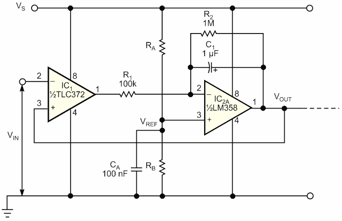
Figure 4 shows a single-supply version of the circuit, in which RA and RB set a reference voltage, VREF, at IC2A's noninverting input, such that IC2A maintains a virtual potential equal to VREF at the inverting input. Thus, when VIN goes more positive than VOUT, the comparator's output MOSFET turns on, pulling the output down to 0 V and impressing a potential equal to VREF across R1. This action, in turn, injects a current pulse equal to VREF/R1 into C1. In most respects, the circuit behaves in the same manner as the circuit in Figure 1. As in the dual-rail version, VOUT cannot go below the potential at the op amp's noninverting input. Therefore, even though VIN need not center on a potential equal to VREF, VIN's positive peaks must exceed VREF for the circuit to work properly.
 |
||
| Figure 4. | For operation from a single power supply, this version of the peak detector sets a reference voltage via resistors RA and RB. |
|
To select a value for VREF, examine the input and output common-mode- voltage ranges of both op amp IC2A and comparator IC1 and the maximum peak-to-peak swing of the input signal. For example, setting the positive power-supply voltage, VS, to 10 V and setting RA = RB sets VREF = 5 V. The detector accommodates an input signal that swings from 0 V to approximately 8 V and thus detects positive peak voltages of 5 to 8 V. Remember to select R1 according to the value chosen for VREF.