A recent project evaluated the feasibility of a dynamic load modulation (DLM) RF power amplifier for 5G. DLM amplifiers typically use high-voltage varactor diodes in their output network, which need to be driven by high-speed large linear voltage pulses.
The pulses needed to have a peak voltage of +80 V and be DC coupled, therefore eliminating the use of a transformer. The circuit also had be to linear in order to accurately recreate the shape of an input pulse at its output. Conventional op amps are incapable of producing large output voltage swings, and certainly not at high frequencies. Although some hybrid modules like those from Apex Microtechnology exist, they have high current consumption and could not meet the project requirements.
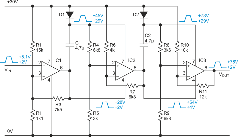
The circuit shown in Figure 1 was inspired by capacitive charge pump circuits [1] that are widely used in power supplies to generate either high voltages or negative voltages. Figure 1 uses op amps instead of switches to achieve linear operation. This design uses three stages, but a greater number could be cascaded to achieve a higher output voltage.
 |
||
| Figure 1. | This analogue charge pump uses op amps instead of switches to achieve linear operation. | |
In theory, it should only take three stages to produce a 90 V voltage swing with a +30 V supply. In practice, however, this is not possible, due to the voltage drop of the diodes and limitations of the op amps’ output stages. The maximum input and output voltages for the LM6171 op amp used in this design must be limited to 2 V below its supply rail voltages to prevent latch-up from occurring. Unfortunately, high-speed op amps capable of full rail-to-rail swings are not currently available for rail voltages >12 V. To accommodate this limitation, voltage drops have been incorporated into the design, which limits the op amps’ output swings to between 6 and 76 V.
In Figure 1, amplifier IC1 has a gain of 8.3 V/V to amplify the input signal to 26 V peak-to-peak. This drives C1 which forms a charge pump with D1. They provide the supply voltage for IC2. Differential amplifier IC2 senses the difference between its own supply voltage and the +30 V supply. When the output of IC1 rises, IC2 detects this and also rises, effectively amplifying the output of IC1 with a gain of 1.9 V/V. Its output swings between 4 and 54 V. A similar operation is performed by IC3 and its associated circuitry. The resistor values were calculated by examining the circuit voltages at the minimum and maximum output voltage swing.
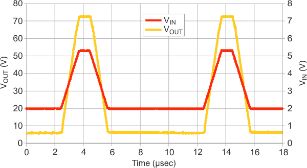
An example result is shown in Figure 2, where the input is a 100 kHz pulse with 1 μs rise and fall time. The output linearly tracks the input to a peak swing of 6 to 72.8 V. As previously mentioned, the circuit was designed for driving varactor diodes, which exhibit a high impedance, hence the current required to drive them was small and well within the capability of the LM6171s.
 |
||
| Figure 2. | Measured input (VIN) and output (VOUT) waveforms of the analogue charge pump. | |
If necessary, output current could be increased by using multiple op amps in parallel. [2] One disadvantage of this design is that the output must remain low for a long enough time for the capacitors to fully charge up so they can supply enough current during the peaks.
References
- Newnes Electronics Circuit Pocket Book, Marston, R., ISBN 0750608579, pp. 159-162.
- “Doubling the Output Current to a Load with a Dual Op Amp,” Renesas Application Note AN1111.