A clock-recovery architecture can operate with NRZ digital signals, even at low SNRs. A clock-recovery subsystem is based on a PLL comprising a phase comparator, a loop filter, and a voltage-controlled oscillator (VCO). If you place the phase comparator after the demodulator block, a typical criterion for comparison is the zero crossings of the received signal (the edges of a TTL-compatible signal). The phase comparator must provide a voltage proportional to the phase difference between the incoming signal and the locally generated clock (the VCO output). But, in comparison with a synthesizer-based phase comparator, the comparison must take place only when information exists; that is, at data-level transitions. The recovery system should disable the phase comparator in the absence of data-level transitions to minimize comparator noise. Figure 1 shows a phase comparator you can implement in a CPLD or an FPGA. Tests show that the comparator works successfully in a 2-Mbps VSAT demodulator with SNR of 6 dB and lower. The comparator can easily acquire and track the signal.
 |
||
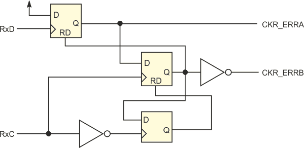
| Figure 1. | A programmable-logic IC forms the phase comparator for the clock-recovery system. | |
The phase comparator uses three D-type flip-flops with asynchronous reset inputs. The comparator has two inputs: RxD and RxC, and two outputs: CKR_ERRA and CKR_ERRB. These inputs and outputs form a three-level output, both high for increasing frequency, both low for decreasing frequency, and both at different levels for no change in frequency. They form a state machine:
- Data rising edge triggers CKR_ERRA.
- Once triggered, next RxC rising edge triggers CKR_ERRB and resets CKR_ERRA.
- Next RxC falling edge (thus, a half-clock period later) resets CKR_ERRB.
 |
||
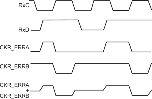
| Figure 2. | The last waveform represents the absolute value of the difference between CKR_ERRA and CKR_ERRB. |
|
 |
||
| Figure 3. | The phase comparator’s output is nonlinear; however, the nonlinearity is inconsequential to the clock-recovery function. |
|
Figure 2 shows the operation of the phase comparator. The transfer function is not linear (Figure 3). It corresponds to the expression
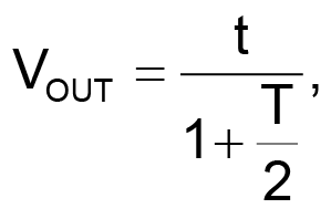
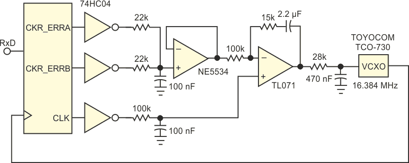
where t is the time from RxD's rising edge to RxC's rising edge, and T is the period of RxC. The nonlinear transfer function is not a limitation, because the system operates around the point at which t=T/2. Moreover, the presence of noise effectively reduces the comparator's gain and smoothes its operation. Thus, the PLL's design must accommodate variations in the comparator's transfer function. Figure 4 shows a simplified final PLL implementation. The programmable-logic device uses buffering to attenuate the digital switching noise of the device. The op amp's noninverting reference input comes from the filtered symmetrical clock signal; thus, the reference level is exactly centered between the low and high logic-level voltages. The system is thus voltage-independent.
 |
||
| Figure 4. | The complete clock-recovery circuit uses a small handful of components. | |