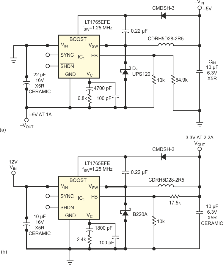
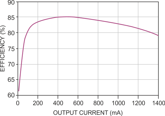
Power-supply designers can choose from a plethora of available positive buck regulators that can also serve as negative boost DC/DC converters. Some buck regulators have a negative-feedback reference voltage expressly for this purpose, but ICs that have positive-reference feedback voltages far outnumber these negative-feedback regulators. You can take advantage of this greater variety of devices by using a positive buck switch-mode regulator to create an excellent negative boost converter. All you need are a few small modifications to the typical buck-converter configuration. Figure 1a shows a –5 V-input to –9-output, 1.4 A negative boost converter using the LT1765EFE positive-buck-converter, switch-mode regulator. This IC accepts 3 to 25 V input, uses a 1.2 V feedback voltage, and has an internal 3 A power switch. The 1.25-MHz switching frequency of the LT1765EFE helps reduce the size of the inductor and input and output capacitors. Figure 1b shows a typical positive-buck-converter application for the LT1765EFE: a 12 V-input to 3.3 V-output, 2.2 A DC/DC converter. Figure 2 shows an efficiency plot for the regulator in Figure 1a.
 |
||
| Figure 1. | The LT1765EFE positive buck converter can make a negative boost converter (a) or a positive buck converter (b). |
|
In Figure 1a, the ground pin of the IC connects to the negative voltage VOUT. This connection makes the negative-boost-converter configuration provide a positive voltage at the FB pin with respect to the ground pin of the IC. In this topology, the maximum input voltage rating of the IC has to be greater than the magnitude of output voltage for the negative boost converter. The IC must also have a minimum input-voltage rating that is less than the magnitude of the input voltage, to ensure that the circuit turns on upon power-up, because the output voltage can have an initial state of 0 V.
 |
||
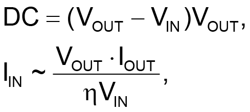
| Figure 2. | Efficiency of the negative boost converter in Figure 1a is as high as 85% and typically greater than 80%. |
|
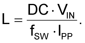
Note that the maximum output current for the negative boost converter in Figure 1a is much lower than the maximum output current of the positive buck converter in Figure 1b, even though they use the same switch-mode-regulator IC. The buck-converter IC in both circuits has an internal power switch with a switch current rating of 3 A. You choose the inductor based on maximum output current, peak switch current, and desired ripple current. First calculate the duty cycle (DC) and then calculate either the ripple current, IPP, based on the chosen inductor, L, or the inductor value based on the desired ripple current. It is generally good practice to choose the inductor value so that the peak-to-peak ripple current is approximately 40% of the input current. These calculations are approximate and ignore the effect of switch, inductor, and Schottky-diode power losses. You calculate as follows:
where η is the overall efficiency.
where fSW is the switching frequency; and
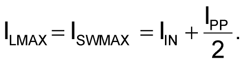
Maximum inductor current, ILMAX, is equal to the peak switch current in this configuration. The IC has a maximum switch current, ISWMAX, of 3 A, so the maximum inductor current must remain below 3 A. To keep switch current below the maximum, you might need more inductance to keep the ripple current low enough.
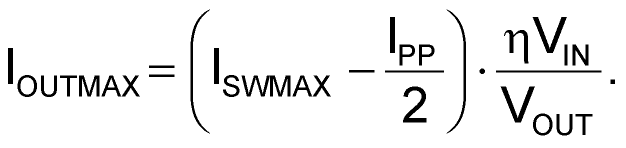
Maximum output current, IOUTMAX, is an approximation derived from the maximum allowable input current given the ripple current:
As in a typical boost converter, the input capacitor in the negative boost topology has low ripple current, and the output capacitor has high discontinuous ripple current. The size of the output capacitor is typically larger than that of the input capacitor to handle the greater rms ripple current:
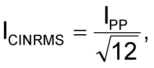
and
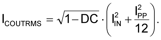
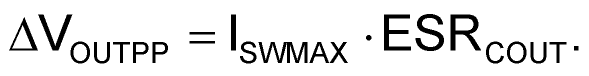
The output capacitor's ESR has a direct effect on the output-voltage ripple of the DC/DC converter. Choosing higher frequency switch-mode regulators reduces the need for excessive rms ripple-current rating. Regardless, a low-ESR output capacitor, such as a ceramic, can minimize the output-voltage ripple of the negative boost converter:
Figures 1a and 1b show the high-di/dt switching paths of the negative boost and positive buck DC/DC converters. You must keep this loop as small as possible by minimizing trace lengths to minimize trace inductance. The discontinuous currents in this path create high di/dt values. Any trace inductance in this loop results in voltage spikes that can render a circuit noisy or uncontrollable. For this reason, circuit layout can be just as important as component selection. Note that the layout of a negative boost regulator differs from that of a positive buck regulator, even though they use the same IC.