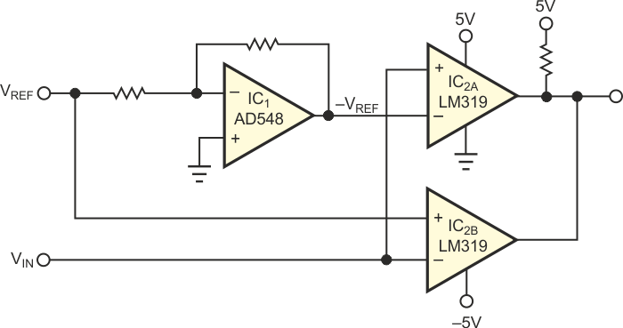
A typical window comparator uses two comparators and a single op amp to determine whether a voltage is inside or outside a boundary region. Figure 1 shows a typical implementation. IC1 is an inverting op amp with a gain of –1. VREF and –VREF create the window limits. When VIN becomes more positive than VREF, the output of IC2A goes low. When VIN becomes more negative than –VREF, the output of IC2B goes low. If VIN is lower than VREF and greater than –VREF, both outputs of IC2 remain high. The LM319 and AD548 come in 14- and eight-pin packages, respectively. The LM319 accommodates separate input and output power supplies. The input supply can be ±15 V referenced to analog ground, and the output can use a logic supply referenced to logic ground. The circuit's input limit is ±2.5 V because of the maximum differential-input limit of the LM319. If you think the input will exceed a ±5 V differential voltage between VREF and VIN or –VREF and VIN, then you must incorporate a clamping network with many additional discrete components. The circuit in Figure 2 overcomes these limitations.
 |
||
| Figure 1. | This traditional window-comparator circuit suffers from limited input range. | |
 |
||
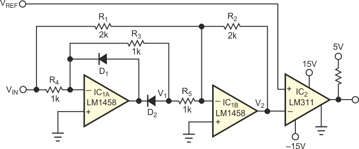
| Figure 2. | An absolute-value comparator circuit offers a wide input range and improved dc performance. | |
To increase the maximum differential-input voltage, you can use an LM311, but it is available only in eight-pin packages, so the circuit would require three eight-pin packages. To reduce the chip count, the circuit in Figure 2 uses an absolute-value amplifier driving a single LM311 comparator, IC2. Although at first glance the circuit in Figure 1 may look simpler than the one in Figure 2, you can save pc-board area and improve performance by using a dual amplifier in a single eight-pin package and an LM311, also in an eight-pin package. In Figure 2, when the absolute value of VIN exceeds VREF, the output of comparator IC2 goes low. When VIN is positive, IC1A inverts the signal, and the voltage at R5 is equal to –VIN. The current flowing through R5 is –2 times that flowing through R1, and the output of IC1B is equal to VIN. When VIN is negative, D2 blocks the output of IC1A, which is clamped to the forward voltage of D1. Because the inverting input of IC1A and IC1B are both at virtual ground, no current flows through R3 and R5. With IC1A effectively out of the circuit, IC1B’s gain is –1, and the output voltage is positive. The inverting-input voltage of IC2 is always at a positive value. This circuit is symmetrical for positive and negative voltages. The following expressions define V2:
V2 = |VIN | = –VIN –(–2VIN)
for positive inputs, and
V2 = –VIN
for negative inputs.
 |
||
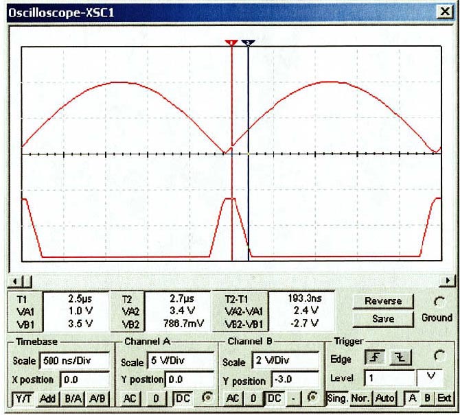
| Figure 3. | Channel A is the rectified (absolute-value) output of IC1B; Channel B is the output of the comparator. |
|
 |
||
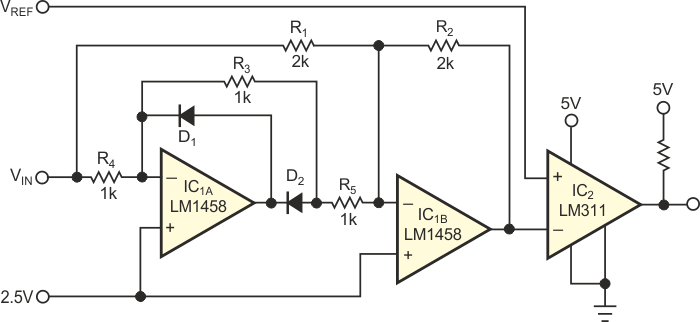
| Figure 4. | You can modify the circuit in Figure 2 to work with a single supply. | |
The dual comparators of Figure 1 can have slightly different thresholds. You can select the dual op amps in Figure 2 for input offsets below 1 mV; doing so allows the circuit in Figure 2 to offer improved dc performance. Another advantage of the circuit in Figure 2 is the fact that you need change only R2 to set the gain of the circuit. Most comparators have offset voltages of several millivolts, so scaling up the input voltage improves accuracy by increasing the signal/offset ratio. The circuit in Figure 1 would require the addition of another op amp to achieve this goal. The simulation in Figure 3 shows the circuit response. Channel A is the output of IC1B. Channel B is the output of the comparator with VREF set at 1 V. Marker 1 corresponds to the 1 V threshold, and Marker 2 corresponds to logic low at the output of the comparator. The circuit in Figure 4 is another variation of the circuit that uses a single 5 V supply. It works for input signals of 0 to 5 V and VREF of 2.5 and 5 V. The 0 and 5 V inputs result in the maximum value of 5 V at the output of IC1B. With VIN at 2.5 V, the output of IC1B assumes the minimum value of 2.5 V.