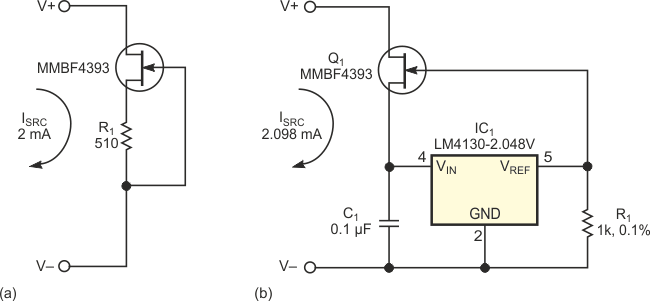
The common JFET current-source in Figure 1a has average output impedance and depends heavily on the JFET's VP and IDSS variations. These manufacturing variations limit the initial accuracy of the current setpoint that the circuit can obtain with a fixed R1. Most users of JFET current-sources sample VP and IDSS for each lot of JFETs and then select R1 by first solving the quadratic equation
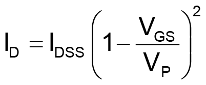
for VGS and then solving the current-setpoint equation
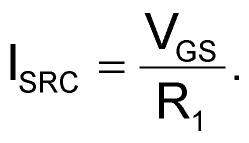
After completing these lot-specific calculations, the accuracy error for ISRC can be less than ±15%. In addition to initial accuracy error at ambient, the VGS overtemperature performance limits the current temperature drift to 0.3%/°C. The temperature dependence of VGS is a function of both the mobility variation of IDSS with IDSS negative-temperature coefficient and the built-in potential of VP’s positive coefficient. VGS has one ID operating point at which it has a zero temperature coefficient, but this one current setpoint is probably not the one that you wanted. With resistors commonly available at 0.1%, 25 ppm/°C grade, R1 will be a small contributor to any errors in the current setpoint. Compliance voltage across the current source is VGS to BVDSS. The output impedance, RO, for this current source is approximately 1 MΩ. You can improve RO to approximately 10 MΩ by adding another JFET in a cascode configuration.
 |
||
| Figure 1. | The common JFET transistor current source (a) has an average output impedance. A composite voltage reference and JFET circuit (b) features higher output impedance, high accuracy, and low temperature drift. |
|
In contrast, the composite circuit in Figure 1b adds an IC voltage reference to the JFET that improves the output impedance. ISRC is set by IC1’s output voltage divided by R1 plus the small ground-current (50 µA) of IC1. The good supply rejection of the LM4130 nulls any VGS variation of the JFET. The current path is from V+ through the n-channel JFET (drain to source) into IC1’s supply input and then out VREF and through R1 to V–. The gate current of Q1 is in the picoamp range. The JFET's VGS, approximately 1.2 V, keeps IC1 biased well above its dropout level.
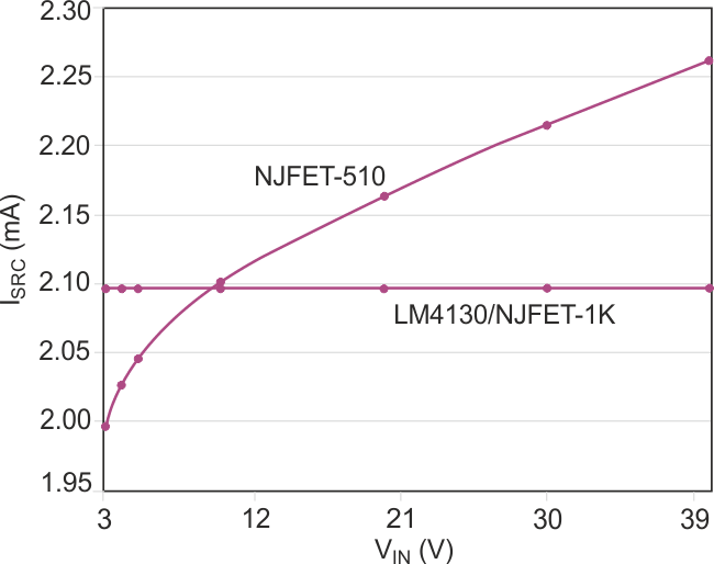
Figure 2 shows ISRC versus VIN of both the JFET and the composite current sources. The slope of these two operating plots represents the inverse of output resistance. The composite circuit curve has an output resistance of greater than 200 MΩ as compared with the JFET-only output resistance of 0.2 MΩ.
 |
||
| Figure 2. | The composite configuration improves the variation of ISRC with a change in VIN. |
|
To a slighter degree than output impedance, the circuit in Figure 1b also improves the initial accuracy of ISRC. The high accuracy achievable with IC1 and R1 controls the setpoint. Both these components are available in at least 0.1% grades. However, IC1’s ground current of 50 µA introduces an offset to ISRC, which you must include in the calculation. IC1’s ground-current variation of ±7 µA is the practical limit of ISRC’s accuracy. Table 1 summarizes the impact on the practical accuracy that you would attain for a range of ISRC values.
| Table 1. | Impact on accuracy for ISRC | ||||||||||||||||||||||||
|
|||||||||||||||||||||||||
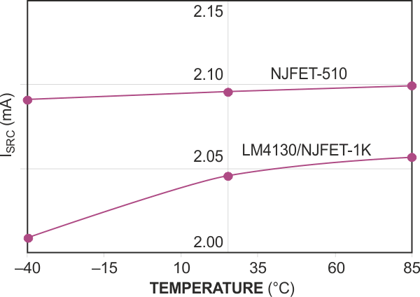
Figure 3 compares the overtemperature performance. Again, IC1’s ground-current variation dominates for ISRC set below 200 µA. IC1’s variation of ground-current overtemperature is ±5 µA.
 |
||
| Figure 3. | The composite configuration also offers a slight improvement in the variation of ISRC with a change in temperature. |
|
The compliance voltage across the composite is VGS + 2.1 V to BVDSS + 5.5 V, or approximately 3.5 to 36 V. Regarding overvoltage stress, when VIN goes above BVDSS + 5.5 V, the composite circuit's setpoint permanently goes into the microamp range due to the CMOS structures within the LM4130 that the overvoltage destroys. The JFET-only configuration may shift the setpoint by 20% but otherwise will be more forgiving of an overvoltage stress. You can further enhance the composite configuration by cascoding the JFET, which boosts the output resistance to approximately 1 GΩ and extends the VIN range to more than 70 V.