A key parameter of capacitors is their dielectric absorption (DA). If you want to estimate the capacitor’s quality or recognize its type of dielectric you can simply measure its DA. This simple circuit can help to avoid the time-consuming standard procedure for choosing a capacitor with proper DA. It can even readily distinguish between polypropylene (PP) and polystyrene (PS) capacitors, which have DA values that are close, without disemboweling the caps to look at the dielectric within.
There are several methods for estimating or measuring the DA value. For a classical direct measurement, the capacitor under test (CUT) is charged (“soaked”), then briefly discharged. The voltage that the capacitor regains after a waiting period is the dielectric absorption voltage (DAV). Standards exactly define the durations for all phases of the process, and the procedure is time-consuming. Another option is to estimate the distortions that DA brings into the work of an RC integrator. You could also estimate the distortions that DA causes in a pure sinusoidal signal on an RC grid. Strictly speaking, the last two methods differ mainly in the measurement procedures involved.
The circuits below are consistent with the requirements of the classical measurement technique. They can maintain timing similar to that of the classical method, which is quite large (on order of an hour), however, the timing can be truncated to several seconds or less.
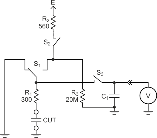
The circuit in Figure 1 contains two reed relays (S1, S2) that control the charge and discharge of the CUT. It also contains a sample-and-hold circuit (reed relay S3 and capacitor C1), which performs sampling of the DAV on capacitor C1. All relay contacts are shown deactivated.
 |
||
| Figure 1. | This circuit can measure dielectric absorption for a capacitor under test by properly controlling the timing of the reed relay switches. |
|
Resistors R1 and R2 limit the charge and discharge currents for the CUT and C1. They should be rated to handle the charging voltage E. Resistor R3 is optional. It may be added if a leak through relay S2’s case is high enough to make non-zero readings when the CUT is disconnected, i.e., CUT = 0.
The sample-and-hold circuit increases the CUT output pulse duration, allowing you to examine it more easily. Because the sampling causes a systematic error, however, you will need to correct the readings by multiplying them by
Capacitor C1 should have a low leakage and low absorption. Most PP, PS, or NP0 ceramics should comply.
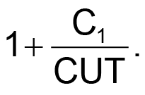
The counter in Figure 2 controls the timing for the switches. A microcontroller could be used to control the timing, but the circuit was chosen to avoid the need for any programming.
 |
||
| Figure 2. | To control the switches in the circuit of Figure 1, a timer activates relay drivers. | |
The timing circuit consists of an oscillator and ripple-carry binary counter (CD4060B) which, together with two 4023 NAND gates, produce the control sequence for the switches (Figure 3). The third gate of the 4023 is not used in the circuit and any unused input of it should be connected to a logic level.
 |
||
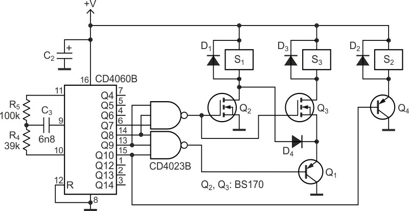
| Figure 3. | This is the timing sequence generated by the circuit in Figure 2. | |
The pairs Q1/Q2 and Q1/Q3 create logical “A-or-notB” and “A-and-notB” circuits, correspondingly. These help to reduce the total number of components and keeps this part of the circuit resistor-less. Specifically, Q3 is used because relays (as with all other switches) are slower to release, than to actuate. Transistors Q1 and Q4 should have enough gain to control the reed relay; in most cases 2N3906, BC560, or BC327 would comply.
The value of voltage V should be sufficient for the relays, while not exceeding the limits of CMOS logic (20 V for “B” grade) and the MOSFET gate-source ratings. The reed relays S1 (SPDT) and S2/S3 (both SPST-NO) should have coil voltages 1 to 2 V lower than +V. The relays should also have low leakage between their terminals; I noticed an issue when the coil-to-contact resistance was in the range of no more than tens of MΩ.
The test cycle time depends on the oscillator frequency and which four 4060′ outputs are used. (These outputs should go in a strict succession, therefore outputs Q12 – Q14 cannot be used.) For the CD4060B shown, with V = 10 V, the clock period (T) is:
Thus, T is about 7 milliseconds (ms), so the test cycle length = 0.007 × 1024, or about 7 seconds.
The time T is not critical and can be lessened ten-fold (or more) by choosing a lower value for C1. This may be especially convenient when testing CUT devices with lower capacitance.
These circuits can be used to estimate the DA of capacitors that are not too small (as low as 10 nF for the components values shown). There is also an upper limit for the capacitance the circuit can test, because CUT may not have enough time to fully discharge if its capacitance is too great.
The discharge time (t) this circuit provides is one half-period of the CD4060 counter’s output Q7. Because the DA for most capacitors is, in the best case, no less than 0.01%, we can estimate the minimal discharge time (t) required for CUT as:
or approximately:

where R1 is the value of the current-limiting resistor.
Hence, if t(Q7) is 70 ms, for a discharge time (t) of 35 ms, and R1 = 300 Ω, then the upper limit for CUT is:
which is approximately 12 μF.
The DAV you will be measuring is roughly proportional to the charging voltage E, so E should be high enough to make DAV noticeable. The relay types and resistor values of Figure 1 will also depend on the value of E.
You can directly measure the DAV estimate using any high-resistance (RI > 10 MΩ) voltmeter connected as shown in Figure 1. A voltmeter with no less than 4.5 digits resolution is preferable because it is possible DAV will be quite small. To have stable readings, however, the voltmeter’s time constant C1 × RI should be much greater than the cycle duration (t). In some cases, this can be a problem, so a scope may be preferable to a voltmeter. In the case when two capacitors of the same capacitance are being compared, the scope can also provide more obvious readings.
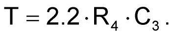
Examples of DA measurements taken with this circuit are shown in Figure 4, using a scope instead of a voltmeter. Results for three capacitors with the same capacitance (CUT = 220 nF) but different dielectrics – polyester film (PET/mylar), PP, and PS – are shown. The scope is set to 10 mV/division and the test circuit parameters were: E = 100 V and C1 = 100 nF.
 |
||
| Figure 4. | Representative DA measurements for three capacitors of the same value clearly show the differences in their dielectric types. |
|
For the PE capacitor, the DAV output pulse amplitude is about 85 mV, for the PP capacitor this amplitude is about 18 mV, and for the PS capacitor it’s only about 9 mV. Thus, the distinction between dielectric types is quite evident.
Calculating the DA value (DAV/E) with the sampling error correction, we get:

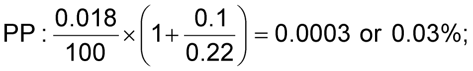
This data is in good agreement with datasheet references.
Safety note
The measurements will continuously repeat while the power is on. When the power is off, the CUT will discharge through the normally closed contacts of S1. Its discharge time depends on its capacitance, however, so if both the capacitance and the charging voltage E are high enough, be certain to obey safety rules when (dis)connecting the CUT. The circuit should be switched-off well before doing so. Also, please observe the proper polarity for electrolytic CUTs.
Final thoughts
Using some stock of capacitors with known capacity and dielectric you can readily calibrate the circuit. Also, it would be a good idea to extend the range of suitable capacitance the circuit can handle by varying the oscillator frequency, i.e., by changing the value of C3. Increasing the value of C3 to 100 nF (or larger) makes the working cycle easily observable, which can help in debugging if a problem occurs. Finally, instead of the 4060, you can use a 4040 chip and supplement the circuit with an oscillator.