Applications ranging from frequency counting and synthesis to sensor signal conditioning require conversion of RF signals to digital-logic levels. In such situations, designers typically use a high-speed voltage comparator to perform the RF-to-digital conversion. Due to their high gain, voltage comparators typically exhibit good sensitivity but also present some drawbacks. High-speed comparators are expensive, difficult to find off the shelf, and prone to rapid obsolescence.
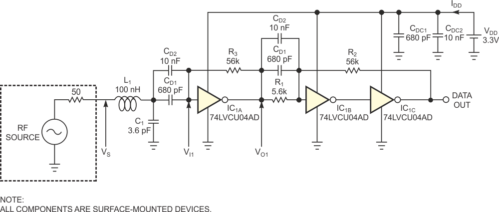
For frequencies as high as 180 MHz, the circuit in Figure 1 offers an attractive approach. The IC in the design, a 74LVCU04 very-high-speed CMOS hex inverter, is available off the shelf and from many sources. Furthermore, many applications may already include three unused inverters. A single inverter, IC1A, operating as a linear preamplifier, forms the converter's input stage. Biasing resistor R3 forces the inverter into its linear region by equalizing its input and output voltages at one-half of the power-supply voltage, VO1 = VI1 = VDD/2. Because the ac gain of a very-high-speed CMOS inverter is relatively low at RF (VO1/VI1) ≈ 7, additional gain stages follow the preamplifier. One self-evident approach – a cascade of additional inverters – presents poor stability at low frequencies and at dc when no RF source is present.
 |
|
| Figure 1. | Three high-speed CMOS inverters and a few passive components form an RF-to-logic converter. |
The circuit in Figure 1 eliminates this drawback thanks to a topology based on a Schmitt trigger and amplifier circuit, IC1B and IC1C, that includes a frequency-dependent positive-feedback network comprising R1, R2, CD1, and CD2. Depending on the input frequency, the network exhibits two behaviors: At high frequencies, the decoupling-capacitor pair, CDC1 and CDC2, short-circuits feedback resistor R1, canceling the time constant introduced by the positive-feedback network, R1 and R2, and the input capacitance of inverter IC1B. Consequently, at high frequencies, the three inverters, IC1A, IC1B, and IC1C, behave as three cascaded, high-speed amplifiers that allow the best performance in input-signal bandwidth. At dc and low frequencies, the influence of coupling-capacitor pairs CD1 and CD2 is negligible, and inverters IC1B and IC1C and the positive-feedback network, R1 and R2, act as a Schmitt-trigger circuit. The choice of the high- and low-threshold voltages, VTH and VTL, at the Schmitt trigger's input, VO1, stems from a compromise between input sensitivity at VS and ensuring unconditional stability of the comparator's output. Equations 1 and 2 set the high and low threshold voltages, respectively:
 |
(1) |
 |
(2) |
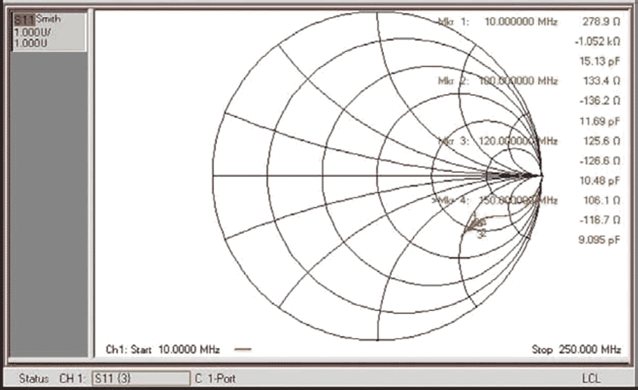
To counteract a roll-off of sensitivity at higher frequencies, add a low-Q impedance-matching network comprising L1 and C1 at the comparator's input. Given the design objective of obtaining acceptable sensitivity at frequencies as high as 160 MHz, the network matches the 50 Ω RF source and IC1A’s input impedance, ZI1, at 150 MHz. Unfortunately, manufacturers of digital ICs typically do not specify logic devices' input impedances. When designing the matching network, the first task involves using an Agilent vector-network analyzer to measure the first inverter's input scattering parameter, S11, at IC1A’s input, VI1. Figure 2 shows a Smith-chart plot of the inverter's S11 parameter.
 |
|
| Figure 2. | An Agilent N3382A vector-network analyzer obtained this S-parameter plot, which shows S11 measured at the first inverter’s input for a source power level of –6 dBm. |
Knowing that
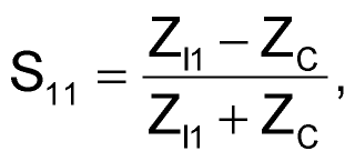 |
(3) |
with ZC = 50 Ω, you can use the data in Figure 2 to extract the first inverter's input impedance at the frequency of interest. At 150 MHz, this yields ZI1 = 106.1 Ω – j116.7 Ω (at Marker 4 in Figure 2). To determine values for the matching network's components, you can use any of several software tools (references 1 and 2). If you are unfamiliar with Smith-chart computations, you can also proceed analytically with the following method:
- Use series-to-parallel transformation formulas (equations 4 and 5) to transform the first inverter's input impedance into a parallel form:
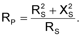 |
(4) |
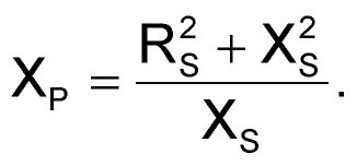 |
(5) |
Applying these formulas at 150 MHz yields: RP = 233 Ω, and XP = 213 Ω. (At 150 MHz, XP represents an input capacitance, CP = 5 pF.)
- Compute an initial version of the matching network to perform a match between the real part of the first inverter's input impedance, RP, and the 50 Ω RF source. Solving equations 6 and 7 yields values for the matching network's elements (Reference 3):
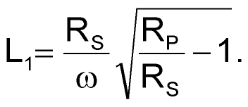 |
(6) |
 |
(7) |
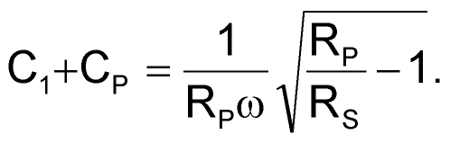
Applying these formulas at 150 MHz yields L1 ≈ 100 nH, and C1 + CP ≈ 8.7 pF.
- Subtract the inverter's input capacitance, CP = 5 pF, from Equation 7 to calculate a value for C1:
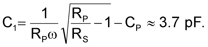 |
(8) |
 |
|
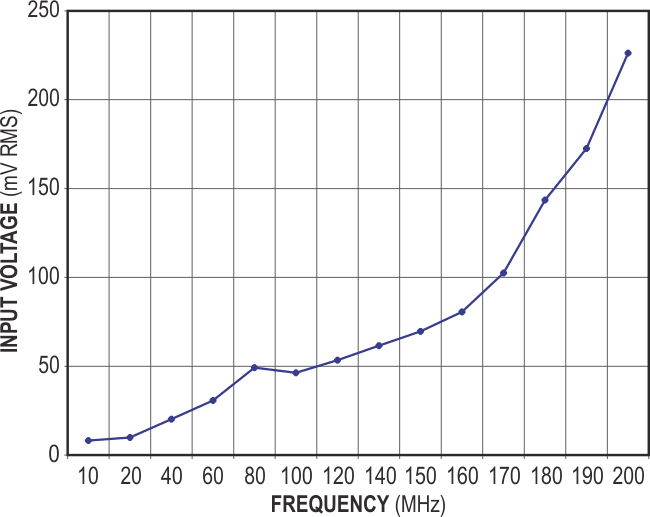
| Figure 3. | An input-level-versus-frequency plot of the RF-to-digital comparator measured from the RF source’s reference plane to a clean logic output reveals less-than-100-mV sensitivity at 160 MHz and usable output to 200 MHz. |
To build the circuit, use standard component values that fall closest to the computed values: L1 = 100 nH, and C1 = 3.6 pF. As the plot of input frequency versus sensitivity in Figure 3 shows, the circuit's increased sensitivity for 100- to 170-MHz frequencies clearly demonstrates the impedance-matching network's effectiveness. You can optimize the circuit's sensitivity in any other frequency band of interest by applying this method at the chosen frequency. The RF-to-digital-logic converter's power consumption does not change significantly for input signals of 10 to 180 MHz. Under worst-case conditions, the current drain does not exceed 58 mA for a supply voltage of 3.3 V.
References
- Smith tool, Ansoft Corp.
- Ansoft Designer: Student Version, Ansoft Corp.
- Bowick, Chris, RF Circuit Design, HW Sams & Co, Indianapolis, IN, 1988.