Class AB amplifiers have been the workhorses of the audio world, thanks to their simplicity, and their ability to deliver high power levels with low distortion. But there are also a number of gremlins that lurk within the AB architecture, mostly in the form of bias instability and other thermally-related issues. I developed this circuit to solve some of the unpleasant shortcomings I encountered with the class AB power amplifier designs while retaining all the virtues that are prized by engineers and audiophiles alike.
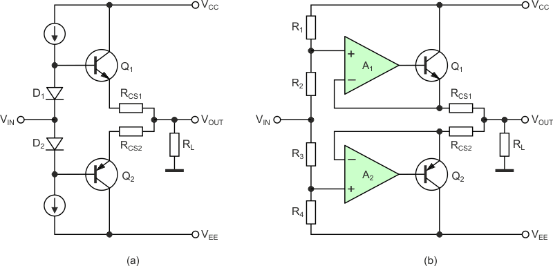
The standard topology of a Class AB power amplifier is shown in Figure 1a. When no signal is applied to the input, a relatively small current flows through the transistors to keep them in amplification mode. This bias current is defined by the voltage drops across diodes D1, D2, the base-emitter junctions of transistors Q1, Q2 and the current-sensing resistors RCS1, RCS2.
 |
|
| Figure 1. | Power amplifier topologies with diode bias (a) and op-amp bias (b). |
The voltage drops across the four PN junctions do not match and they all depend on temperature. Bias current is somewhat hard to define and current adjustment is often required. To minimize these thermal effects, the amp’s diodes and transistors must be in close thermal contact to provide normal biasing at varying output power.
The circuit in Figure 1b solves the bias problems. Since there are no temperature-dependent components in the loop formed by R2, A1, RCS1, RCS2, A2 and R3, the bias current can be precisely calculated and it does not depend on temperature. The schematic cited in Reference 1 used that topology to build a 2-W audio amplifier with good performance.
 |
|
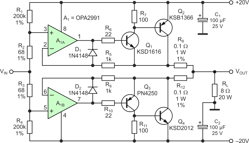
| Figure 2. | This current booster circuit delivers up to 20 W of power and exhibits a well-defined temperature- independent quiescent current. |
This Design Idea (see Figure 2) pushes the improved topology to the power limit.
The key is OPA2991, a rail-to-rail I/O op amp capable of working with a ±20 V power supply. Using small current-sensing resistors and two pairs of complementary transistors to provide larger currents, the circuit can deliver up to 20 W of power to an 8-Ω load with modest quiescent current, low distortion and wide bandwidth. Unlike traditional Class AB designs, its bias current does not depend on temperature and no adjustment is required. Diodes D1 and D2 are on when transistors are not conducting so the op-amps are always in active mode.
The amplifier’s performance data underlines the advantages of its improved architecture:
- Input resistance is 100 kΩ; it does not depend on frequency
- When VIN = 0, the output voltage is about 10 µV and the circuit draws 60 mA from the power supplies
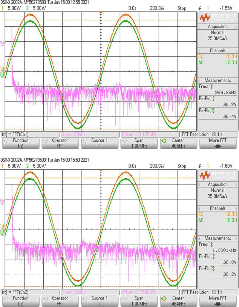
Figure 3 shows VIN (the orange trace), VOUT (the green trace) and their spectrums at maximum power and 1 kHz.
 |
|
| Figure 3. | VIN and VOUT at maximum power and 1 kHz. The upper graph shows the spectrum of VIN, the lower graph shows the spectrum of VOUT. |
Other key takeaways:
- The transfer coefficient is 0.99
- The power delivered to the load is 20.4 W
- The circuit draws 700 mA from the power supplies
- Transistors Q2 and Q4 dissipate about 4 W of power each, requiring appropriate heat sinks
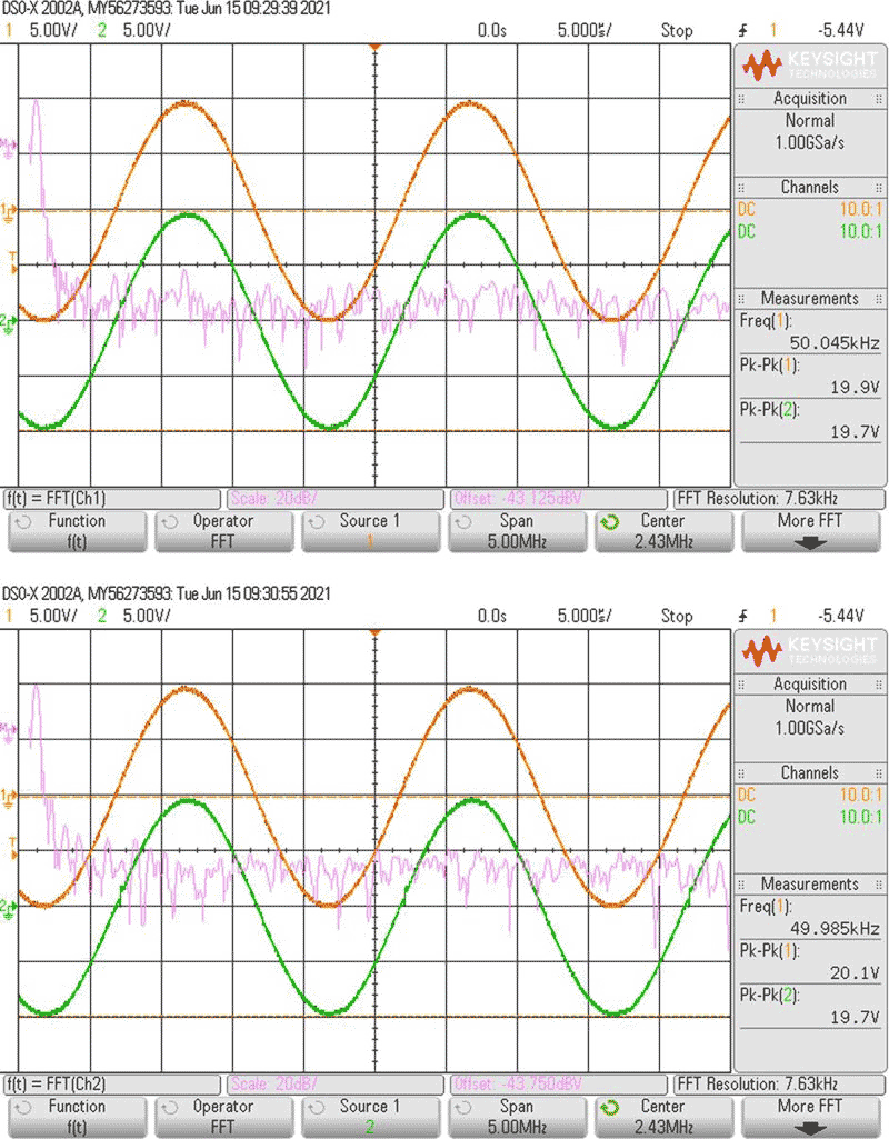
Simulation shows that the circuit has significant bandwidth and low distortion. At 1 kHz, the noise floor is about 80 dB below the fundamental peak. The two spectrums are pretty identical, which means the circuit introduces no distortion. Simulation reports a total harmonic distortion (THD) of 0.021%. Figure 4 illustrates these features at 50 kHz.
 |
|
| Figure 4. | VIN, VOUT and their spectrums at 50 kHz. |
At 50 kHz, the noise floor is about 60 dB below the fundamental peak. The noise portions of the two spectrums are pretty identical. Close to the fundamental peak (the first box in the graphs), the output spectrum is slightly higher than the input spectrum; this means the circuit introduces some distortion there. Simulation shows THD = 0.216%.