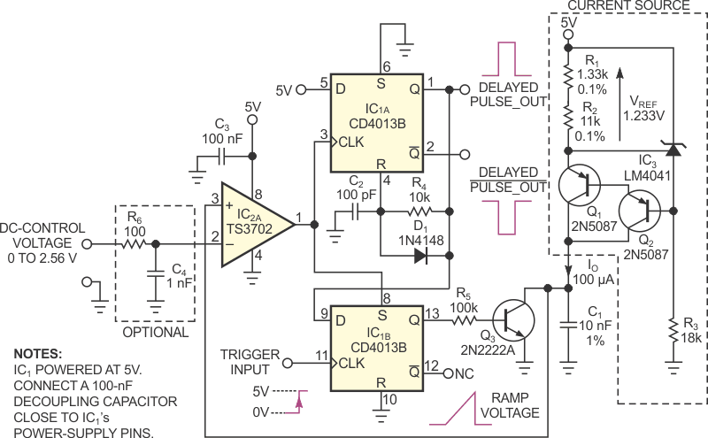
Some applications require clock-timing adjustments, such as generating precision clocks for time-interleaved ADCs, or delay adjustments in a variety of precision-timing and pulse-delay applications. This Design Idea describes a delayed-pulse generator using a dual-CMOS D-type flip-flop (Figure 1). The circuit provides precision time delays of a trigger-input pulse. A dc-control voltage selects a time delay within the full-scale range. When the rising edge of a pulse triggers the input, the circuit’s output generates a pulse with its rising edge delayed by an amount equal to the selected time delay, TD, plus a fixed inherent propagation delay TPD. Also, a time constant, R4C2, determines the output pulse’s width.
 |
|
| Figure 1. | The rising edge of a trigger input starts a precision ramp voltage that compares with a control voltage, generating a precise delay. |
A precision dc source, IO, and capacitor C1 set the full-scale delay range. When Q3 is off, the current source charges capacitor C1, generating a linear-ramp voltage with slope equal to IO/C1. The delay is the time it takes for the ramp to rise from its initial voltage to the control-voltage value.
In this application, the ramp slope is 10 mV/1 µsec, so that the full-scale delay range is 256 µsec for a control voltage of 0 to 2.56 V. You can set the full-scale delay by changing IO through either R1 + R2 or capacitor C1. For best accuracy, the current source can range from 10 µA to 1 mA, the capacitor’s value can range from 1 nF to 1 µF, and the corresponding full-scale delay can range from 2.56 µsec to 256 msec. Use a precision film capacitor for C1.
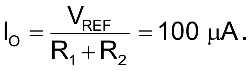
The basis of the current source is a shunt precision-micropower-voltage-reference, IC3, producing a reference voltage of 1.233 V with an initial accuracy of 0.2%. The LM4041, through precision resistors R1 and R2, biases the Darlington-coupled transistors Q1 and Q2 with a reference current
The Darlington configuration ensures that base current is negligible and that the output collector current can achieve a worst-case accuracy of 0.3%. You can use any small-signal transistor, but, for best accuracy, use high-gain, low-level, low-noise BJTs, (bipolar-junction transistors) such as a 2N5087 or a BC557C. IC1A is a one-shot circuit (Reference 1). The output pulse’s width is
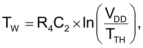
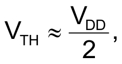
where VTH is the threshold voltage of the digital CMOS. Because
then

Diode D1 reduces recovery time. After power-up, Q3 is in saturation, absorbing the current source’s output, and, as soon as an input pulse triggers the circuit, IC1B’s Q output goes low, switching off Q3, starting a ramp. When the ramp exceeds the control voltage, then the IC2A comparator’s output goes high, and the rising edge triggers one-shot IC1A and switches on Q3 through IC1B, allowing the discharge of the capacitor C1. When an input pulse triggers the circuit, any other trigger pulse that occurs before the falling edge of the delayed output pulse does not produce an output pulse; in other words, the circuit is not retriggerable. This feature permits you, at the same time, to divide and delay an input-trigger clock.
Although IC1 and IC2 can operate from a 3 to 16 V supply, the minimum supply voltage of the circuit is 5 V; otherwise, Q1 and Q2 approach saturation, generating to a less linear ramp voltage. Voltage comparator IC2A, an TS3702, has an input-common-mode-voltage range that includes ground, permitting you to monitor input voltages as low as 0 V.
However, for correct operation of the circuit, the minimum control voltage must be greater than the saturation voltage of Q3. For the components in Figure 1, the measured value is 12 mV. If you want to reduce this voltage, you can use a digital N-channel MOSFET with low on-resistance. The optional input lowpass filter, comprising R6 and C4, helps to clean noise from the dc-control voltage.
If a DAC drives the control input, you can build a digitally programmable delay generator. A suitable low-cost, 8-bit DAC is the AD558, which features an internal precision bandgap reference to provide an output voltage of 0 to 2.56 V, making 1 LSB equal to 1 µsec. It operates from 5 to 16 V, with a 1-µsec settling time. The circuit’s quiescent current, IDD, is less than 300 µA because all ICs are micropower.