When processing signals from analog sensors, you frequently encounter wide variations in attenuation among communication channels or sensors. Or, you face situations in which several identical sensors within a supervised system return signals of roughly similar spectral composition and dynamic range but with considerably different maximum amplitudes. Sometimes, it's possible to predict these and other variations and adjust the gain of preprocessing amplifiers. More frequently, you encounter unpredictable signals and thus lose data associated with nonrepeatable events. In these circumstances, an adaptive preamplifier with AGC (automatic gain control) can prevent measurement-channel saturation and data loss.
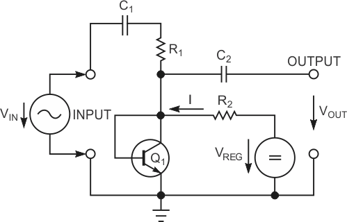
AGC preprocessing suppresses the absolute amplitude of a sensed signal while preserving the best possible resolution of individual spectral components' relative amplitudes. The circuit in this Design Idea offers one relatively simple and efficient approach to per-channel AGC. The circuit uses a method of direct low-level signal control using a short-circuited bipolar transistor. In Figure 1, a variable voltage divider comprising a fixed resistance, R1, and a variable resistance controls the signal's ac amplitude. The variable resistance comprises the differential resistance of a bipolar transistor, Q1, short-circuited from base to collector. To vary Q1’s resistance, you force direct current into the shorted transistor from a current source comprising voltage source VREG and a high-value resistor, R2. To prevent R2 from affecting the circuit's ac-voltage-transfer characteristic, R2’s resistance must greatly exceed R1’s.
 |
|
| Figure 1. | A short-circuited bipolar transistor forms one element of a basic attenuator circuit. |
For all reasonable values of positive current I – generally, less than the transistor's maximum rated emitter current (IE) – transistor Q1’s collector-to-emitter saturation voltage is less than its base-emitter threshold voltage, and the transistor operates in the active state. The shorted transistor's VI (voltage-versus-current) characteristic curve strongly resembles that of a PN diode and follows Shockley's Equation except for slightly higher dc-voltage values. That is, the device's voltage variation is proportional to the logarithm of the dc-current variation.
Therefore, the shorted transistor's differential resistance at every dc operating point along the VI curve is inversely proportional to the passing dc current; in other words, the device's differential conductance is directly proportional to the current. Because, in its active state, a common-emitter-connected bipolar transistor's current-amplification factor is typically 100 or more, the differential resistance accurately follows this rule over a broad range of currents.
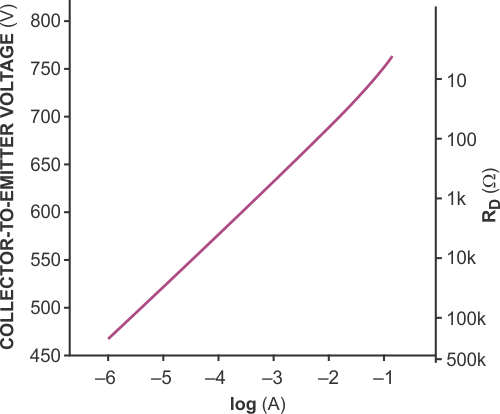
Thus, varying VREG in Figure 1 varies the current, I, and controls the R1-Q1 voltage-division ratio. Coupling capacitors C1 and C2 separate the circuit's attenuator from the input-signal source and output load. Figure 2 illustrates a typical small-signal bipolar transistor's short-circuited VI characteristic, showing that you can control differential resistance over at least five decades of range – that is, more than 100 dB.
 |
|
| Figure 2. | A VI characteristic shows the corresponding differential-resistance graph for a short-circuited BC337-16 transistor. (Note: The -16 denotes a sorted hFE range of 100 < hFE < 250.) |
In a practical circuit, the finite values of R1 and R2 limit the control range. For proper operation and to keep the signal's THD (total-harmonic-distortion) factor, k, below 5%, the output-voltage amplitude, VOUT, should be just a few millivolts. Even with these limitations, this attenuator circuit appears to offer one of the best and simplest AGC circuits.
 |
|
| Figure 3. | You can assemble this AGC circuit entirely from discrete components. |
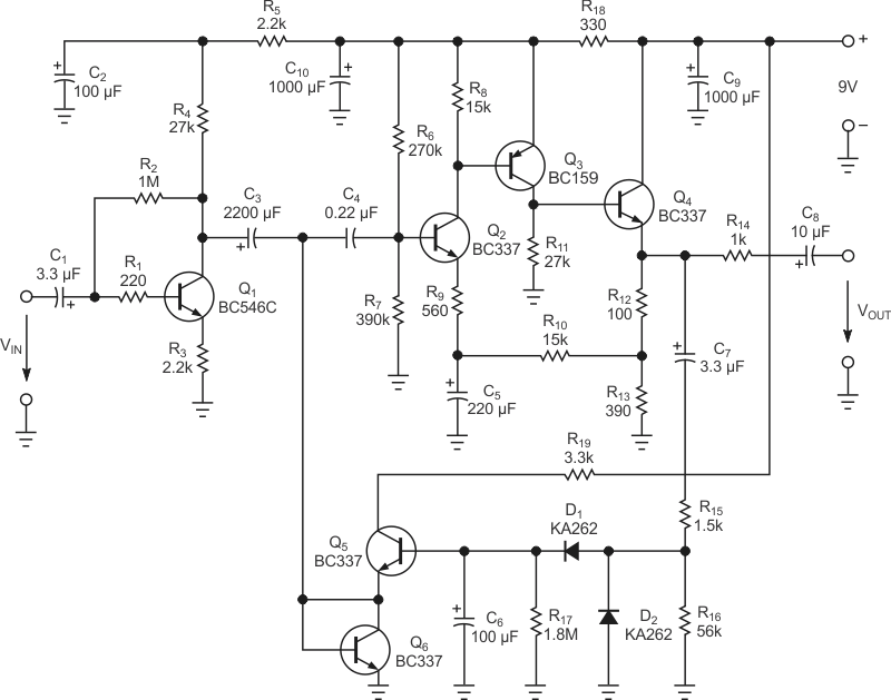
Figure 3 shows the completed circuit design. The input signal, VIN, drives buffer stage Q1, whose unbypassed emitter resistor, R3, serves four purposes. First, it increases Q1’s differential output resistance to the approximate value shown in Equation 1:
 |
(1) |
The increase in the circuit's differential output resistance is so large that the value of R4, 27 kΩ, almost exclusively determines the overall output resistance. Second, leaving R3 unbypassed reduces Q1’s voltage gain to:
 |
(2) |
This equation simplifies to
Note that DhE denotes the determinant
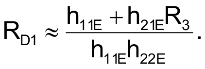
which this Design Idea includes for theoretical accuracy. However, you can neglect the numerical value of DhE for modern silicon transistors without significantly affecting the calculation's accuracy. Third, as Equation 2 shows, leaving R3 unbypassed helps linearize the response of Q1’s collector current-to-voltage drive. Fourth, Q1’s differential base input resistance rises to:
which is larger and less dependent on Q1’s instantaneous operating point than h11E alone.
In Figure 3, resistor R4 forms the variable attenuator's fixed resistance, analogous to the upper resistor, R1, in Figure 1, and Q6 forms the attenuator's variable-resistance element. Transistor Q5 supplies Q6’s collector-drive current, and Q5’s common-emitter configuration draws little base current. This approach enables use of a high value for AGC-release time-determining resistor R17, thus permitting a long AGC-release time. Resistor R19 limits the maximum dc control current through Q5 and Q6.
The large value of C3, when you compare it with Q6’s minimum differential resistance – that is, its maximum signal amplitude – at full control, presents negligible reactance to the lowest frequency-signal-spectrum component. A voltage-doubler rectifier comprising D1 and D2 extracts a portion of the signal from output stage Q4 and produces the control voltage for Q5. This arrangement accommodates both polarities of large peak amplitudes of nonsymmetrical signal waveforms. Resistor R15 determines the AGC's “attack” time. Too small values of R15 in combination with C6 can lead to instability by creating a pole in the feedback-transfer function. Resistor R17 determines the AGC-release time.
To secure good response to high-frequency-signal components, use either Schottky or fast PN silicon diodes for D1 and D2. The dc-coupled complementary cascade comprising Q2 and Q3 supplies most of the circuit's voltage gain. A 1-kΩ resistor, R14, isolates Q4, the output-emitter follower, from the signal-output terminal. If necessary, you can use a lower resistance at R14, but a large-capacitance connecting cable can provoke Q4 into parasitic oscillation if R14 is too low.
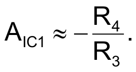
Figure 4 shows the circuit's input-versus-output characteristics as measured with a sine-wave signal. The effective AGC range extends from 100-µV- to 100-mV-rms input voltage, a 60-dB dynamic range. Output voltage varies less than 2 dB over this input range, reaching a nominal level of 775 mV rms at a –20-dB- (100-µV-rms) input level. The input's 0-dB point is set arbitrarily at 1-mV-rms input, which corresponds to an 803-mV-rms output. The AGC attack time for a sinusoidal-input-signal step from 0 to 100 mV rms is approximately 0.3 sec, and the AGC release from 100-mV-rms input to –20 dB (100 µV rms) is approximately 100 sec. Figure 4 also includes a graph of THD versus input voltage. The distortion is well below a 5% THD limit throughout the input-voltage range.
 |
|
| Figure 4. | The circuit’s input-versus-output characteristic shows a 60-dB control range (upper trace) and total harmonic distortion well below 5% over the control range (lower trace). |
To measure the attenuator's baseline input noise, terminate the input with its nominal 1-kΩ source resistance. At low input voltages, input stage Q1’s noise limits the processed signal's usable dynamic range. The rms noise level is about –38 dB relative to the nominal output for input signals below the AGC threshold. When the AGC becomes active, the SNR increases in proportion to the AGC reduction. For example, with a 0-dB- (1-mV-rms) input signal, the SNR increases to approximately 60-to-1.
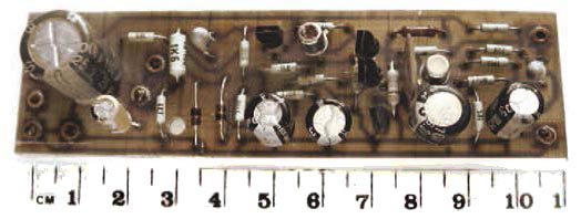 |
|
| Figure 5. | The circuit’s input-versus-output characteristic shows a 60-dB control range (upper trace) and total harmonic distortion well below 5% over the control range (lower trace). |
If you assemble the circuit using the passive-component values in Figure 3, the amplifier's –3-dB bandwidth spans 45 Hz to 35 kHz. At a power-supply voltage of 9 V, no-signal current consumption is approximately 12 mA. Figure 5 shows a photograph of the assembled pc board.