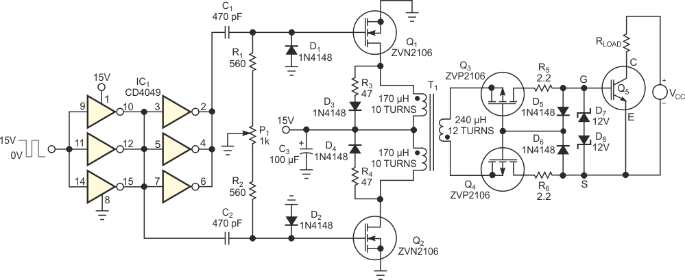
Three-phase controlled rectifiers and inverters, matrix cycloconverters, and cascaded power stages typically comprise large numbers of power transistors, each with its own driver circuit. The circuit in Figure 1 drives a capacitive-input power device, such as a MOSFET or an IGBT (insulated-gate bipolar transistor) with pulses of all duty cycles at frequencies of 1 to 200 kHz. A single transformer provides galvanic isolation, and the circuit consumes little power from its 15 V primary-side power supply. Tested satisfactorily using several MOSFETs and IGBTs with input capacitances as high as 5 nF, the driver can accommodate higher current power transistors by resizing the driver's transistors and coupling transformer and a few passive components.
 |
|
| Figure 1. | The isolated pulse driver transmits all duty cycles and consumes energy only during the gate charge and discharge processes. |
Transistors Q1 and Q2 transmit pulses of approximately 1-µsec duration through coupling transformer T1 to transistors Q3 and Q4, which respectively charge and discharge power transistor Q5’s gate-source input capacitance. The charging pulse that Q1 produces begins on the rising edge of the drive-control signal, and the discharge pulse that Q2 produces begins on the falling edge of the control signal. Differentiator circuits comprising C1, R1, a portion of potentiometer P1, C2, R2, and the remaining portion of P1 set the durations of the charge and discharge pulses. If necessary, adjusting P1’s setting alters the balance of the positive and negative charge and discharge voltages that Q5’s gate receives.
Transistors Q3 and Q4, respectively, transmit pulses to charge or discharge Q5’s input capacitance and then switch off, producing a high impedance across Q5’s input capacitance so that Q5’s gate voltage doesn't change, except for discharging slowly due to small leakage currents. Thus, the driver circuit consumes power only during the short intervals of the gate-to-source charge and discharge processes.
When transistors Q1 through Q4 switch off, resistor and diode pairs R3, D3, R4, and D4 form a path for transformer T1’s demagnetization current. Although they're reverse-biased most of the time, diodes D5 and D6 form a peak-amplitude discriminator, configured as a logical-OR circuit, to ensure that gate voltages at Q3 and Q4 always equal or exceed the voltage at the positive terminal of Q5’s gate-to-source capacitance.
Resistors R5 and R6 limit charge and discharge rates for Q5’s gate-to-source capacitance and can vary depending on Q5’s drive characteristics. Transformer T1 comprises a Philips RM5/I core of 3E5 ferrite material with a center-tapped, 20-turn primary winding and a 12-turn secondary winding, both fabricated from 0.2-mm-diameter, 0.008-in, AWG #32 magnet wire.
When transistor Q1 switches on, it induces a positive voltage in T1’s secondary winding that switches on P-channel MOSFET Q3 and drives Q4’s internal body diode into conduction to begin charging Q5’s gate-to-source capacitance. Q3’s on-channel resistance primarily determines the charging rate. Charging ends either when the pulse terminates or when Q5’s gate-to-source voltage approximates T1’s secondary voltage minus Q3’s gate-threshold voltage.
Next, Q3 switches off, allowing the charging current to decay to zero and the capacitance to reach its maximum positive charge. When Q1 switches off, transformer T1’s magnetizing current resets through R3 and D3. The voltage at T1’s secondary winding goes slightly negative to balance the core's volt-second characteristic, which forward-biases Q3’s body diode without current, and Q4’s body diode blocks the discharge of Q5’s gate-to-source voltage.
The negative voltage you apply to Q4’s gate cannot switch on Q4 because diode D5’s forward-voltage drop sets Q4’s gate voltage higher than the voltage at Q5’s gate. Thus, Q5’s input capacitance remains charged, and the reset path presents high impedance to this capacitance. When Q2 switches on, the negative voltage that appears on T1’s secondary turns on Q4 and starts the discharge process, which ends when Q4’s source-to-gate voltage equals its threshold level or when the pulse terminates. Then, Q4 turns off, and Q5’s gate-to-source capacitance reaches its minimum negative voltage. When Q2 turns off, T1’s magnetizing current resets through D4 and R4, Q4’s body diode conducts, and Q3’s body diode blocks Q5’s gate-to-source voltage. Diode D6 applies a high voltage to Q3’s and Q4’s gates to ensure that the reset voltage at T1’s secondary doesn't drive Q3 into conduction. Thus, all transistors remain off, and Q5’s gate-to-source capacitance remains discharged.
 |
|
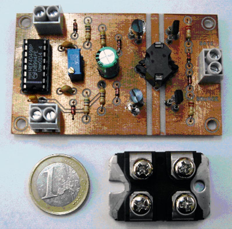
| Figure 2. | A top view of the isolated gate driver’s prototype version shows that an isolation barrier interrupts the ground plane beneath transformer T1 (upper right center). |
When Q1 next switches on, the sequence repeats.
 |
|
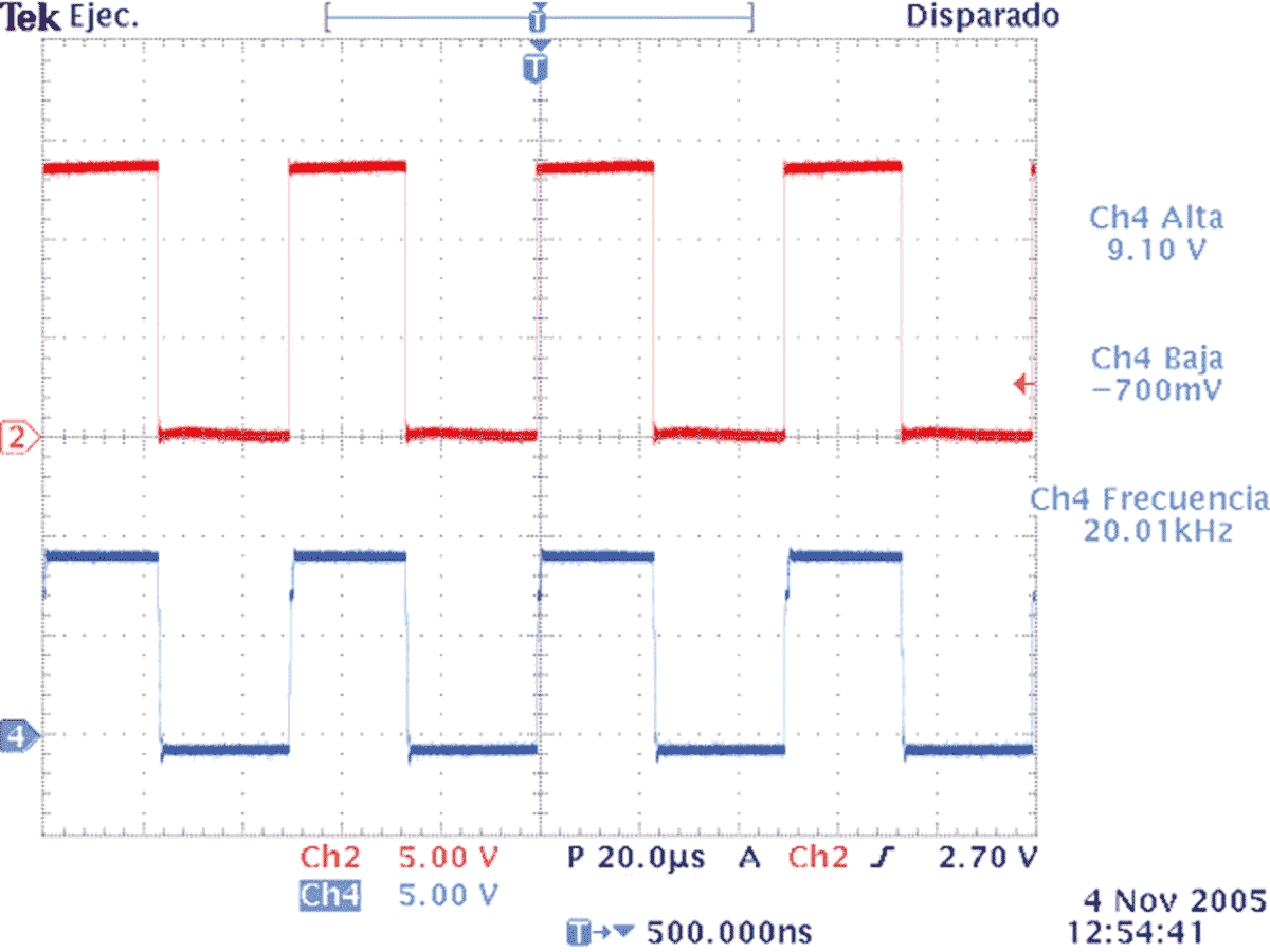
| Figure 3. | The top trace shows the driver-control voltage, and the bottom trace shows the gate-source voltage of an APT40GF120JRD IGBT, Q5, at 20 kHz. You can use potentiometer P1 to adjust the 9.1 and 20.7 V high and low gate-to-source levels, respectively. |
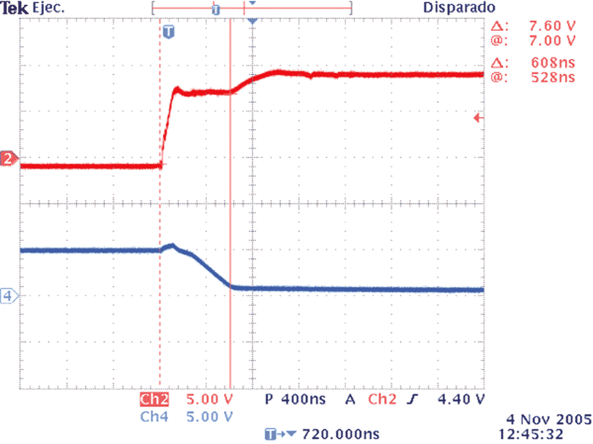
Figure 2 shows the driver prototype compared with a €1 coin and a power transistor. The transistor, APT40GF120JRD, combines an IGBT and a FRED (fast-recovery epitaxial diode) that operates at a maximum of 1200 V and 60 A with a gate-to-source capacitance of 4 nF. The transistor comes in a JEDEC SOT-227 package measuring approximately 1.5 × 1 in. (38 × 25 mm). Figure 3 and Figure 4 show experimental waveforms for the circuit of Figure 1 to drive IGBT Q5 at 20 kHz. The turn-on delay is approximately 600 nsec, and the total current consumption is 22 mA for a power consumption of 0.33 W. When driving transistors that present a lower gate-to-source capacitance, the circuit's turn-on delay and power consumption both decrease.
 |
|
| Figure 4. | The top trace shows the driven transistor’s gate-to-source voltage, and the bottom trace shows its collector-emitter voltage, which a probe attenuates. The transistor’s load comprises a resistor that connects to a power supply. |