The circuits of PWM pulse generators with independent frequency and duty cycle adjustments are described. The first one uses the TLC555 IC and an external master pulse generator on the CD40106 IC. The second oscillator is made on the D-trigger of the CD4013 IC and the analog comparator LM339.
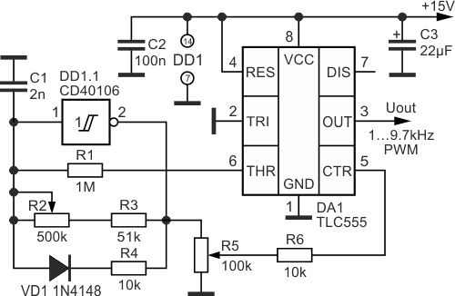
The 555 chip, well known to radio amateurs, allows you to generate a PWM signal, but the frequency of such a signal changes markedly with a change in the width of the output signal. It is possible to solve the problem of creating a PWM generator with independent adjustments and using a 555 chip, for example, TLC555 or its equivalent, using an external master pulse generator.
The square wave generator with independent frequency and pulse width adjustments, Figure 1, produces a PWM signal at the output in the frequency range from 1 to 9.7 kHz. The master oscillator is made on the DD1.1 element of the CD40106 IC. The operating frequency of the generator can be smoothly adjusted by potentiometer R2.
 |
|
| Figure 1. | PWM generator with independent frequency and pulse width adjustments. |
On the capacitor C1, sawtooth pulses are formed, slowly rising in time and quickly falling off by the end of the pulse. These pulses are sent to pin 6 of the DA1 TLC555 IC. From pin 5 of the DA1 IC, the signal through resistor R6 is fed to the potentiometer R5, which provides smooth adjustment of the width of the output pulses taken from pin 3 of the DA1 IC.
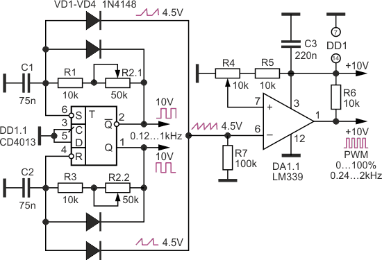
Figure 2 shows a oscillator circuit for a similar purpose, made on the D-flip-flop DD1.1 of the CD4013 IC and the analog comparator DA1.1 of the LM339 IC.
 |
|
| Figure 2. | A variant of a square wave oscillator with independent frequency and pulse width adjustments. |
The master oscillator of the device is assembled on a D-trigger DD1.1 and it works by adjusting the dual potentiometer R2.1, R2.2 in the frequency range from 0.12 to 1 kHz. The amplitude of the output signals of a rectangular shape at the outputs 1 and 2 of the IC reaches the supply voltage, i.e. 10 V.
On the time-setting capacitors C1 and C2, a sequence of sawtooth pulses with an amplitude of 4.5 V is formed with an inter-pulse pause of 50% of the pulse duration. These pulses through the diodes VD1 and VD4 1N4148 are summed up on the resistor R7 and fed to the input of the comparator DA1.1 LM339 (pin 6). The other input of the comparator (pin 7) receives a comparison voltage from a resistive divider made on resistor R5 and potentiometer R4.
Potentiometer R4 allows you to adjust the pulse duty cycle from 0 to 100% within the frequency range of the output signal from 0.24 to 2 kHz, i.e. twice the frequency of the master oscillator signal.
The amplitude of the output signal of a rectangular shape taken from pin 1 of the DA1.1 chip is almost equal to the supply voltage of the device (10 V).