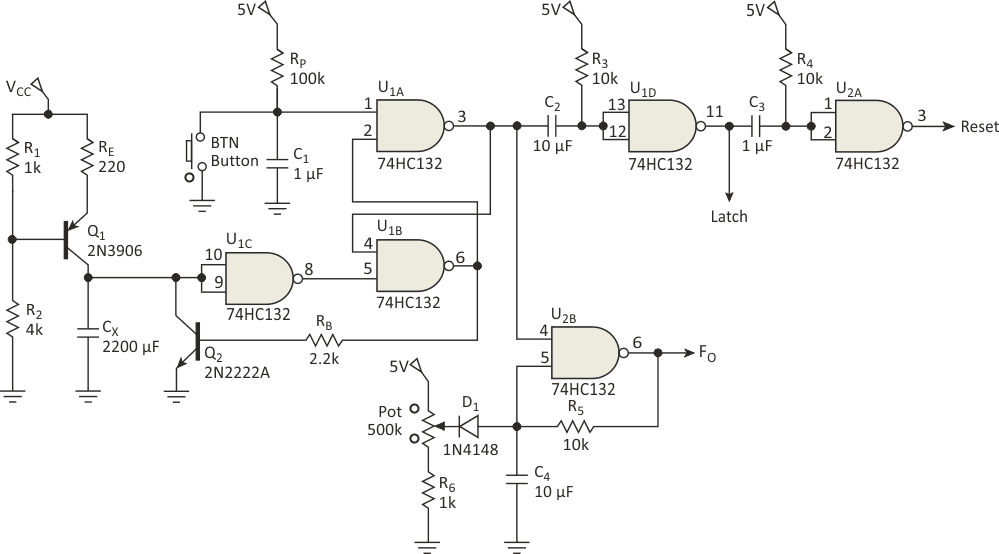
The circuit in Figure 1 allows you to convert capacitance into a pulse train by using a constant current source and a linear monostable formed by two NAND-gate chips (74HC132). The circuit also provides two pulses to control external counter functions such as Latch and Reset, which are normally required by digital counters and latches when driving a display. Applications for the monostable include instrumentation circuits when the need arises to convert a transducer’s capacitance measurement (such as relative humidity), into a pulse train.
 |
|
| Figure 1. | Capacitance to pulse-train converter based on Schmitt-trigger NAND gates. |
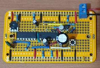
CX represents the capacitance transducer (Fig. 1, again).The circuit is triggered by a N.O. pushbutton, which has a debouncing network formed by RP and C1 to create a clean transient Low pulse. Figure 2 shows the actual assembled circuit on a printed circuit board (PCB). A 0.1-µF bypass capacitor is placed between voltage and ground.
 |
|
| Figure 2. | Assembled circuit on a PCB using 1% tolerance resistors. |
In its initial state, U1B is high, driving transistor Q2 in saturation, which keeps capacitor CX grounded (Fig. 3). This disables the gated oscillator formed by U2B.
 |
|
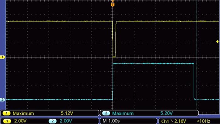
| Figure 3. | Trigger pulse and the Q output on gate U1A. |
When the pushbutton is pressed, the SR latch makes U1A go high while U1B goes low (Fig. 4). This puts transistor Q2 in cutoff, allowing CX to charge linearly with a constant current.
 |
|
| Figure 4. | Trigger pulse and the output from gate U1B (in blue color), which puts transistor Q2 in cutoff. |
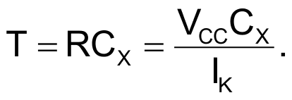
The constant current source is formed by Q1, a PNP transistor, and its associated components. This constant current IK is defined by Equation 1:
 |
(1) |
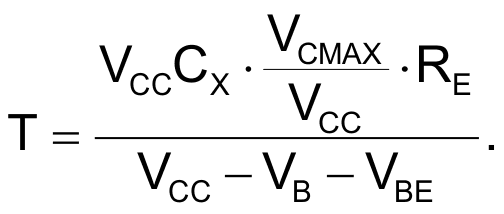
where VCC = 5.1 V, VB = 4.1 V, and VBE = 0.7 V. To get the timing constant T, we substitute the current IK in variable R as follows in Equation 2:
 |
(2) |
Equation 2 is then multiplied by the ratio (VT+/VCC), which is defined by the positive threshold voltage in NAND gate U1C and VCC. This ratio represents the maximum voltage that capacitor CX will reach. By substituting IK in Equation 2, we get a linear timing and charging ramp (Fig. 5) with its respective Equation 3:
 |
(3) |
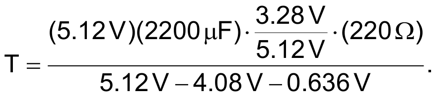
Then we substitute our component values and voltage measurements to get Equation 4:
 |
(4) |
When capacitor CX = 2200 µF is placed, for example, we get a time period equal to 3.9 seconds. The accuracy of this result depends on the tolerance of all the components contained in Equation 4.
 |
|
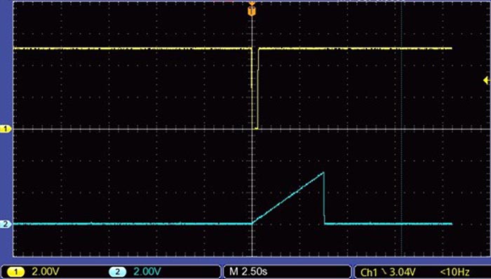
| Figure 5. | Trigger pulse and voltage ramp on capacitor CX. |
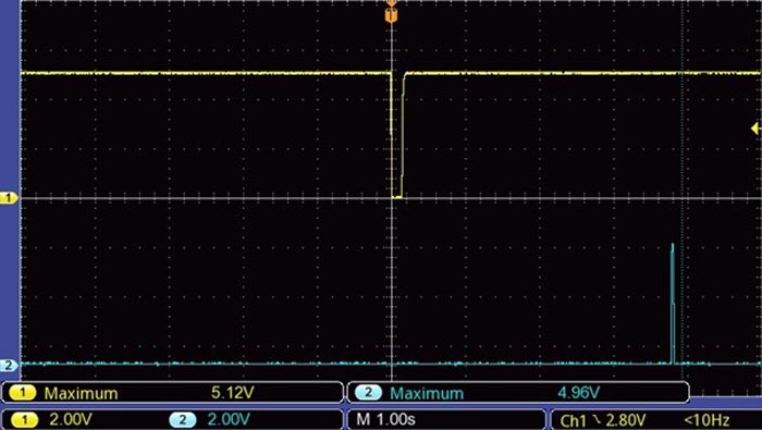
The constant current IK stops charging capacitor CX when its voltage reaches the positive threshold voltage VT+, in this case 3.28 V. At this point, NAND gate output U1C goes to a logic low, disabling the oscillator, and generates two transient pulses in sequence with the half-monostables formed by NAND gates U1D and U2A.
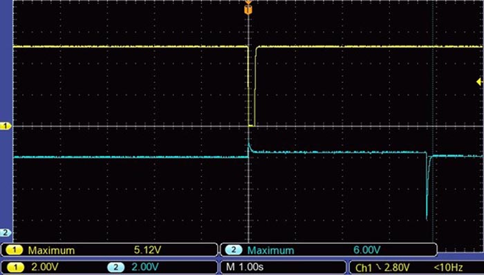
The edge detector formed by U1D is triggered at the falling edge (Fig. 6) from the output pulse coming from NAND gate U1A.
 |
|
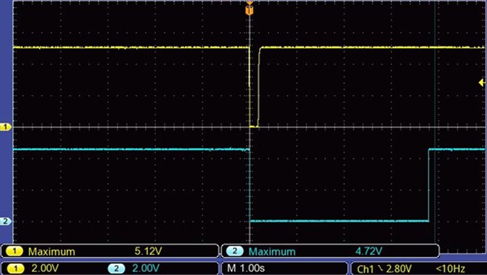
| Figure 6. | Trigger pulse and capacitor’s voltage on VC2 that produces a Latch pulse. |
The positive transient pulse produced by NAND gate U1D is called Latch (Fig. 7), and its period T2 is given by Equation 5:
 |
(5) |
When this pulse ends, it triggers the second half-monostable formed by R4 and C3, producing a positive transient Reset pulse T3 (Fig. 7, again) defined by Equation 6.
 |
(6) |
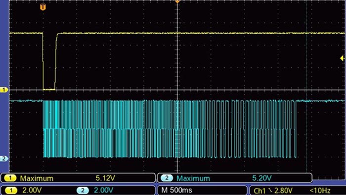
The gated logic oscillator formed by NAND-gate U2B and its associated components delivers a pulse train (Fig. 8) at a frequency defined by Equation 7:
 |
(7) |
where VT– is the negative threshold voltage.
 |
|
| Figure 7. | Trigger pulse and Reset output generated by gate U2A. |
This oscillator doesn’t have a startup delay because the 500k trimpot in series with R6 must be calibrated a few millivolts below the positive threshold voltage VT+ (see reference 1). Notice that when this oscillator is disabled, capacitor C4 requires a time delay to again reach the fixed voltage set by the trimpot. This time delay may vary depending on the capacitor’s voltage before it was disabled. If the capacitor’s voltage was equal to VT− when it was disabled, it will require a recovery time defined by Equation 8:
 |
(8) |
This delay sets the time you must wait to apply the next pulse on the pushbutton. The oscillator frequency is set with a fixed capacitor C4 and resistor R5 according to the counter resolution and desired precision reading. You can add a series potentiometer to R5 to adjust such a frequency.
 |
|
| Figure 8. | Trigger pulse and output frequency on the gated oscillator. |
This circuit can be made to retrigger by itself. A feedback loop would be placed from the Reset pulse to the pushbutton input, using another edge detector triggered at the falling edge. This would require the edge detector to provide a Low pulse on the trigger input with a minimum period equal to 1 µs. RP would not be required. Bear in mind that when triggered by itself, the external counter will keep changing its readings continuously at a rate given by Equation 3. A display must update its readings within one to four times per second; otherwise, it will appear as flickering.
It’s recommended to use 1% tolerance metal film resistors to get variations of up to 1% due to changes in temperature. With respect to the capacitors, you must use polyester or polystyrene types to have minimum value changes with respect to temperature. In addition, the trimpot for R5 must have a low temperature-coefficient constant.
Reference
- “Gated Oscillator Starts Without Delay,” Electronic Design.