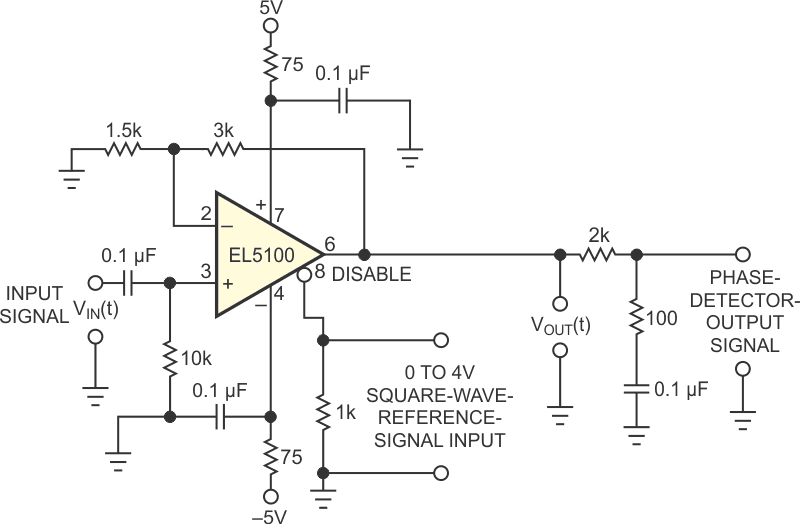
Some op amps, such as the AD8041 from Analog Devices and the EL5100 from Intersil, provide a disable pin, which allows you to parallel the outputs of several op amps for video multiplexing. In addition to this multiplexing, you can also use the disable function to configure the op amp as a phase detector or a frequency mixer. Figure 1 shows how the disable function can implement a low-frequency phase detector. You can switch the gain of this circuit’s amplifier on and off at the rate of the phase-reference signal. Doing so produces a dc component at the output of the op amp. This component is proportional to the cosine of the phase difference between the phase of the input signal and the phase of the reference signal.
 |
|
| Figure 1. | By switching the disable input of the op amp at a reference frequency and lowpass-filtering its output, you can obtain a dc voltage proportional to the phase difference of the switching frequency and the input frequency. |
In the circuit, the output of the op amp is:
where
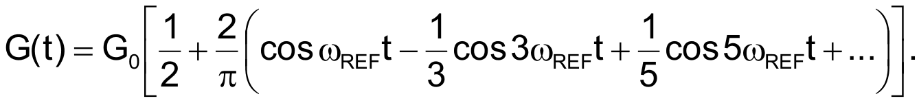
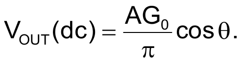
and G(t) is the time-varying gain of the op amp. G(t) is a 50%-duty-cycle square wave that switches from zero to G0 at the frequency of the phase-reference signal. G0 is the gain of the op amp when the op amp is enabled. Because G(t) is a time-varying periodic function expand it in a Fourier series:
Multiplying VIN(t) by G(t) and retaining only the dc terms, the dc component of the output is
The EL5100 op amp in Figure 1 has a 200-MHz unity-gain bandwidth, and you can turn its output on and off by applying a square wave of at least 0 to 4 V to the output-disable terminal, Pin 8. Using the feedback resistances shown and with G0 = 3, the peak output voltage of the phase detector is approximately equal to the peak value of the input signal. The EL5100 has a disable time of 180 nsec and an enable time of 650 nsec, which allows you to gain-switch the device to approximately 250 kHz. At higher frequencies, the gain of the phase detector falls off because the gain-switching no longer has a 50% duty cycle.
The lowpass filter following the op amp extracts the dc component of VOUT(t) and has a 3-dB point at 800 Hz. A 100 Ω resistor in series with the 0.1-µF shunt capacitor limits the phase lag of the filter when the phase detector is inside a PLL (phase-locked loop). The values in Figure 1 provide a maximum phase lag of approximately 65°. Using 5 and –5 V power supplies allows the output swing of the phase detector to be symmetric at approximately 0 V. If your design doesn’t require this symmetry, you can use a single 5 V supply with 2.5 V positive offset-biasing of the op amp. In this case, the output swing is symmetric with respect to 2.5 V. As with all wide-bandwidth-op-amp circuits, you should take care to connect the power-supply bypass capacitors to ground with short connections and as close to the op amp’s power-supply pins as possible to avoid instability.
This same gain-switching scheme also works as a frequency mixer. If the input signal is at frequency ωS and the reference-square-wave input is at frequency ωLO, the IF output signal is (ωLO – ωS) or (ωLO + ωS). You obtain the desired IF signal by replacing the output lowpass filter in Figure 1 with a bandpass filter tuned to the desired IF frequency of ωLO ± ωS. If the switching rate for the reference signal is higher than the disable function can provide, then you can use the harmonic mixing using the odd-order harmonics of the reference signal. This approach reduces the gain of the mixer by a factor of 1/N, where N is the number of the harmonic you are using.