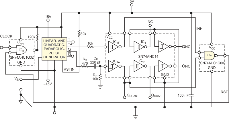
The circuit in Figure 1 is an edge-triggered monostable circuit, based on a previous design of an edge-triggered parabolic-pulse generator (Reference 1). This circuit involves a simple but significant modification of the earlier generator by disconnecting the input comprising IC3 and S2 (in the original design) of the first of the integrators of a cascade from the source of the reference voltage, VREF, and connecting it to the input-voltage terminal in Figure 1.
 |
|
| Figure 1. | A low-to-high transition at the clock input triggers the monostable. The width of the generated pulse at the complementary Q and /Q outputs is a mathematically defined nonlinear function of the analog input voltage of 0 to 3 V. |
The width of the output pulse at output Q in this circuit is
where
and τIL and τIQ are time constants of the first and the second integrators in the cascade comprising Reference 1’s IC2D and IC2C, respectively.
Although the monostable would be functional with just this modification, the logic circuitry of IC1, IC2, and IC3 of Figure 1 adds another feature. The added logic ensures that the generator ignores the next trigger pulse that comes within the monostable’s busy state.
In this way, the generator’s integrator capacitors can discharge close to 0 V with an error not exceeding 0.4%, even at relatively high trigger frequencies, exceeding the value of 1/[TQ(VIN)]. Consequently, the output pulses at a given input voltage are of constant width, even when the triggering period closely approaches or is smaller than the width of the output pulse.
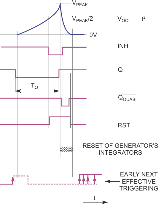
The subcircuit comprising IC1 and IC2 generates an RST (reset) signal, the trailing edge of which determines the end of one cycle of operation of the monostable. The RST signal in this circuit inhibits retriggering of the monostable within the interval in the Q output’s low-to-high transition and the RST signal’s high-to-low transition. For this purpose, the triggering signal’s clock is ORed in IC3 with the RST signal (Figure 2).
 |
|
| Figure 2. | The high level of the generated RST-logic signal prevents any eventual low-to-high transitions at the clock input from triggering the monostable until the integrators of the generator reset in a defined way. |
The next effective triggering is thus enabled just after the trailing edge of the RST pulse. The leading edge of the RST pulse occurs roughly when the quadratic-parabolic voltage, VOUTQ, reaches half its peak voltage, VPEAK. The trailing edge of the RST pulse is delayed with respect to the instant of VOUTQ’s dropping below VPEAK/2. The auxiliary time constant, (RD+RS)CD, of the RS/CD/RD network at the input to IC1A defines this delay.
Experimental evaluation shows that the relative error of the output pulse width,
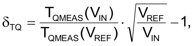
is negative, not exceeding –8×10⁻⁴ for an input voltage of approximately 200 to 3000 mV, with a reference voltage of 3000 mV, which Reference 1’s IC1 sets.
The error then rises in magnitude, reaching a maximum of δTQ = –2.337×10⁻³ at an input voltage of 99.925 mV. By further lowering the input voltage, the negative error decreases in magnitude and is δTQ = –1.113×10⁻³ at an input voltage of 9.915 mV. At an input voltage of 3.08 mV, the relative error is positive, δTQ ≈ 2.9×10⁻³. Further decreasing the input voltage causes the positive error to rise rapidly, reaching 3% at an input voltage of 1.065 mV. Note, however, that the input-voltage span is almost 3000-to-1. The trigger frequency is 2 or 200 Hz.
You can obtain almost the same pulse widths at trigger frequencies of 2 kHz, 200 kHz, and 2 MHz. The relative change of pulse width due to trigger-frequency variation is comparable to δTQ values or lower. A full-scale input, with the input voltage equal to the reference voltage, achieves a measured pulse width of 445.44 µsec.
With the VOUTQ output, you can also use the circuit as a precision quadratic-parabolic-timebase generator; the input voltage controls the generator’s speed.
Reference
- Štofka, Marián, “Positive edges trigger parabolic timebase generator”