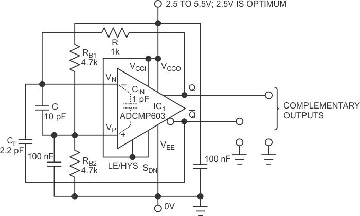
A previous Design Idea describes an astable multivibrator that gets hysteresis from the positive feedback stage using a technique you can characterize as positive-capacitive feedback (Reference 1). It creates hysteresis by a charge transfer to its main timing-capacitor. The circuit uses two logic inverters to generate complementary logic outputs. In contrast, the circuit in Figure 1 uses a single fast analog comparator that has complementary outputs, thus eliminating the need for an additional inverter.
 |
|
| Figure 1. | This pulse generator produces time-aligned complementary logic waveforms. The duty cycle holds at 50%. |
Comparators such as ADCMP603, IC1, have symmetry that results in a very low time skew of the transitions at its Q and /Q outputs that are fractions of a nanosecond. Thus, the charge transfer to the main capacitor, C, theoretically starts immediately at the start of the level transition at the Q output, from which C is charged through a resistor, R. No additional propagation delay occurs at any stage besides Q, resulting in a further increase in operating frequency.
The output frequency of the pulse generator in Figure 1 is less sensitive to supply voltage variations than a generator with the ADCMP603, which uses the IC’s internal hysteresis. The charging current of C and the charge-transfer- based hysteresis of the pulse generator rise almost linearly with the rising supply voltage, which results in an output signal’s insensitivity.
Contrarily, the internal hysteresis, which an external resistor sets at the comparator’s LE/HYS pin, varies nonlinearly with the supply voltage. If, for example, the external resistor’s value is 225 kΩ, the hysteresis has the same value of about 36 mV for supply voltages of 2.5 and 5.5 V.
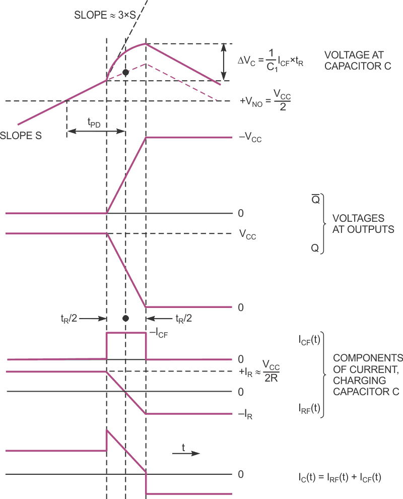
At frequencies close to the upper frequency limit of operation, the charge injection through capacitor CF is gradual rather than steplike because the rise and fall times of waveforms at the Q and /Q outputs are still of finite value. Figure 2 shows an idealized operation for the positive peak of voltage at capacitor C. Although the real voltages, VQ and V/Q, have somewhat rounder “corners,” they resemble those in the figure.
 |
|
| Figure 2. | An idealized but still close-to-reality modeling of the operation of the generator gives you a formula for determining the output frequency. |
If you assume that the voltage swing at capacitor C is considerably lower than that at Q and /Q, then a rectangular current pulse, ICF(t), charges capacitor C during a positive-voltage transition at output /Q. The current through resistor R, IRF(t), which also flows to capacitor C, changes its polarity at the midtransition at Q and /Q outputs. The final current, which charges capacitor C, is a sum of IRF(t) and ICF(t). Although the waveshape of the voltage at capacitor C depends on the final charging current, it gains in peak solely due to ICF(t).
The following equation calculates the added peak:
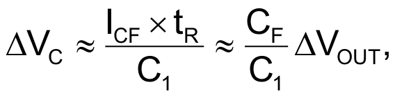
where ΔVC is the added peak, C1 = C + CIN, and C1 ≈ 1 pF. The added peak is independent of IRF(t) due to the zero mean value of this current within the level transition at the Q and /Q outputs.
For C = 10 pF, C1 = 11 pF, CF = 2.2 pF, and ΔVOUT ≈ 2.4 V, a voltage you derive from the equation ΔVC 0.48 V.
The following equation calculates the nearly constant part of IRF(t) current:
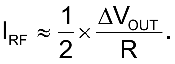
IRF determines the slope, S, of the VC(t) waveform in Figure 2, which excludes the time interval of level transitions at the comparator’s Q and /Q outputs. You calculate the slope with the following equation:
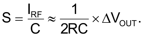
The following equation determines the absolute value of peak voltage of VC(t), referred to supply midvoltage:
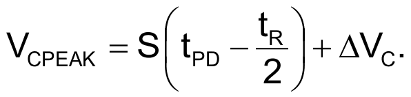
Voltage VC(t) decreases from its peak value with a slope of –S. You calculate the time interval, TDESC, when it reaches the reference level as:
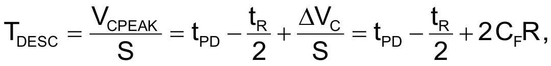
By evaluating this equation for a tPD of approximately 3.5 nsec and R with a value of 1 kΩ, the time interval is approximately 6.8 nsec.
The following equation calculates the total time, when VC(t) is higher than the reference voltage, VCC/2:
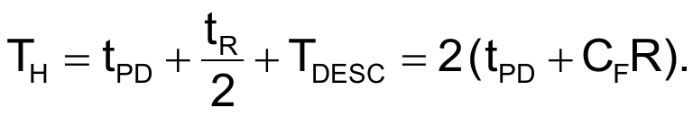
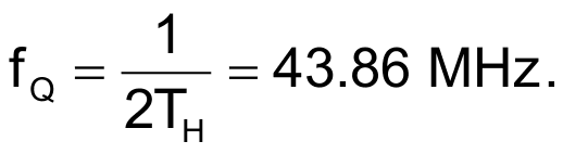
The symmetry of the ADCMP603’s internal circuit architecture, TH, is the right half-period of logic waveforms at the Q and /Q outputs. In other words, the duty cycle of the output pulse is 50%. By evaluating the equation for TH, you get 11.4 nsec. Thus,
The circuit’s output frequency is 56.75 MHz with a power-supply voltage of 2.052 V. With a supply voltage of 3.51 V, the frequency changes to 56.12 MHz. Thus, the relative sensitivity of the output frequency to the supply-voltage variation is approximately 8×10⁻³/V. You can attribute an increase of experimental frequency as compared with a theoretical value to the fact that, during the estimated signal-propagation delay, tPD, the comparator’s input overdrive rises gradually to about 330 mV, which is more than triple the value at which you define the propagation delay. You can therefore assume a lower propagation delay and a higher frequency.