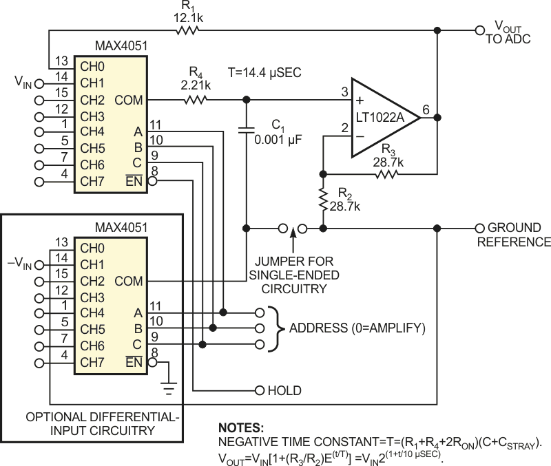
ADCs need adequate signal-acquisition analog interfaces to perform at their best. The classic general-purpose ADC front end includes multiple channels of differential input, digitally programmable gain, and track-and-hold capability. This Design Idea presents a new, complete, high-performance, low-parts-count ADC front end that implements the standard ensemble of functions (Figure 1). However, it also incorporates the concepts of the flying-capacitor differential input and the divergent-exponential negative-time constant that an earlier Design Idea describes (Reference 1). This Design Idea adds to that circuit multiplexed inputs and a versatile track-and-hold function.
 |
|
| Figure 1. | This high-performance, low-parts-count ADC front end implements the standard ensemble of functions. |
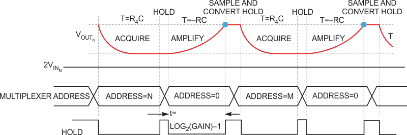
The multiplexer address and the state of the hold-mode bit control signal acquisition and conditioning. With a hold state of zero and the multiplexer’s address equal to the selected input channel, the flying capacitor, C1, connects to the positive and negative differential-input terminals, which acquire the input voltage. Moving the hold state to one isolates C1 from the input. Then, the multiplexer’s address becomes zero, and the hold state returns to zero, initiating regenerative negative-time-constant exponential amplification of the input voltage. From that point until the point when hold reasserts and a connected ADC samples and converts the output voltage, the input voltage and the output voltage are divergent exponential functions of time, with a gain equal to 2(1+t/10 μsec).
 |
|
| Figure 2. | Only the resolution of the amplify interval’s timing limits gain-set resolution. |
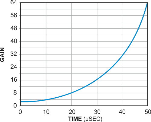
Building on the assets of that earlier design, this new circuit has the desirable features of multiple instrumentation-style differential inputs. Also, neither resistor matching nor the CMR (common-mode rejection) of the op amp limits the circuit’s CMR. Stray-capacitance issues do have an effect on CMR, but you can minimize this capacitance by careful circuit layout. The circuit also has rail-to-rail inputs and virtually unlimited programmable gain. Further, only the resolution of the amplify interval’s timing limits gain-set resolution (Figure 2 and Figure 3). This circuit also has ±10 V output-amplitude capability – two to four times greater than that of monolithic digitally programmable-gain instrumentation amplifiers.
 |
|
| Figure 3. | This graph of input- and output-voltage gain shows the time elapsed since the track/amplify-logic transition. |
The inherent noise and dc accuracy of the chosen op amp, the accuracy and repeatability of the timing of exponential generation, ADC sampling resolution, and RC-time-constant stability are the main limits on signal-processing performance and the amplifier’s precision – for example, its gain-programming accuracy, dc error, noise, and jitter. In the circuit, 1 nsec of the amplify-interval timing error or jitter equates to 0.007% of gain-programming error.
Reference
- Woodward, W Stephen, “Flying capacitor and negative time constant make digitally programmable-gain instrumentation amplifier,” EDN, Feb 5, 2009, pg 48.