In a previous Design Idea, a circuit switches precision dc reference voltages to the noninverting input of a high-speed IC comparator (Reference 1). The circuit uses a 2-to-1 multiplexer that functions in a BBM (break-before-make) fashion. Multiplexers have a parasitic capacitance, whose injection of charge, QD1INJ, into the D1 drain electrode of the multiplexer might cause error voltages at the comparator’s reference input (Figure 1). The following equation defines the approximate peak error voltage:
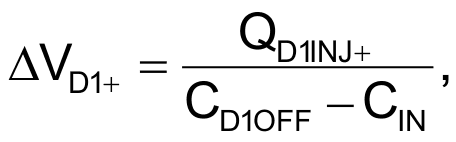
where CD1OFF is the capacitance of the D1 terminal of IC2, and CIN, approximately 1 pF, is the input capacitance of the comparator. IC2 has a BBM interval of approximately 3 nsec, and any Analog Devices ADCMP608 and ADCMP609 comparators’ signal-propagation delays are 10 times that value. Hence, they cannot change their state in 3 nsec. Analog Devices has 10-times-faster parts, the ADCMP601 and ADCMP602, in the same family. Unfortunately, these devices can sense these spikes. The voltage excursion over the high-level reference voltage, VREFH, can result in an abrupt short-term elevation of the output voltage.
 |
|
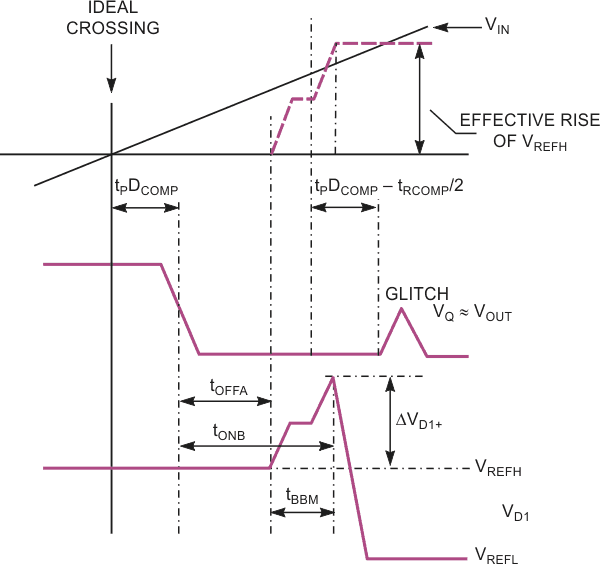
| Figure 1. | Charge injection can produce a glitch in a voltage comparator’s output, and these glitches can cause logic hazards. |
When the high reference voltage exceeds the voltage at the comparator’s inverting input, its output goes high again, or generates a glitch. As the comparator crosses an ideal level, the comparator’s output goes low with a delay. The positive error voltage starts to evolve with an additional delay of the turn-off time of Channel A of IC2. The ADCMP601’s data sheet shows a charge injection into the source electrode. In this case, however, charge injection to the drain electrode plays a role. As a rough estimate, you can use the data on charge injection in Reference 2. As the charge injection changes its sign, depending on the value of the common-mode voltage, the charge is about 0.8 pC at VD1, which equals the high-level reference voltage, and it is approximately –0.3 pC when the reference voltage is low. This voltage ceases with the delay of the turn-on time of the channels in analog switch IC2, an ADG772. The inadvertent return of the comparator’s output to high, although lasting no more than 5 nsec, might cause some logic circuits to respond unexpectedly. A similar situation might occur when the input ramp with a negative slope crosses the lower reference voltage.
 |
|
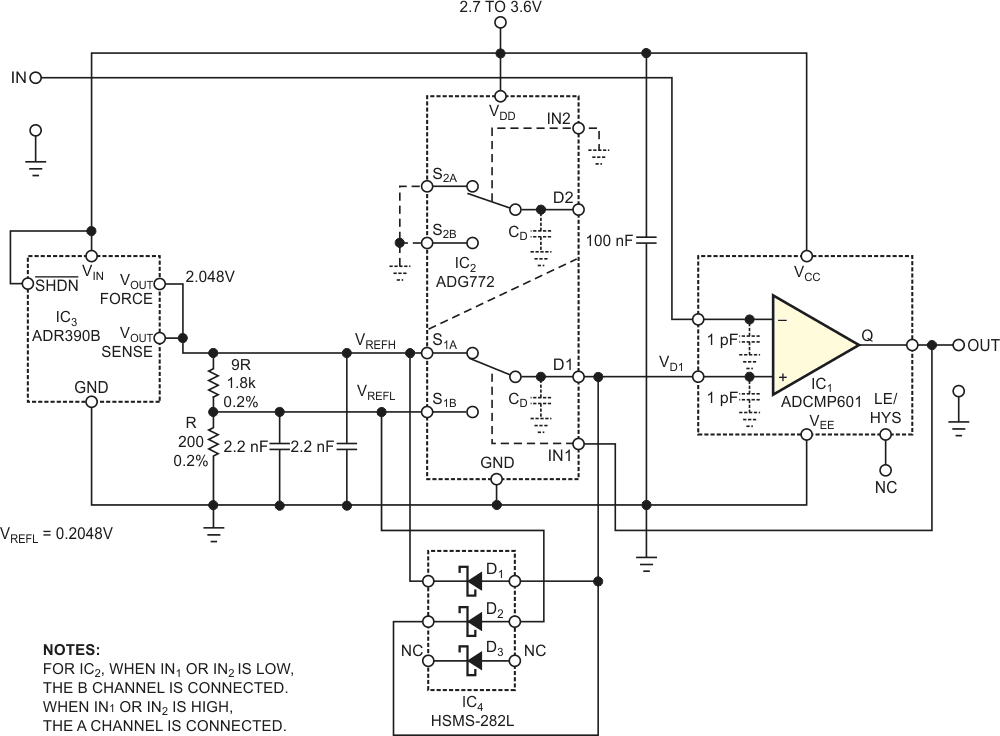
| Figure 2. | Schottky barrier diode D1 damps positive voltage spikes that occur at the noninverting input of comparator IC1 shortly after the high-to-low transition of the output voltage. Diode D2 clamps the negative excursion of the reference voltage during a low-to-high transition of the output voltage. |
To prevent these hazardous states, you can add two Schottky barrier diodes (Figure 2). Diode D1 starts to conduct whenever a positive voltage excursion of approximately 200 mV above the higher reference voltage occurs at the D1 terminal, whereas D2 conducts at excursions of 200 mV below the lower reference voltage. Further, the nonlinear junction capacitance of these diodes rises with forward voltage from 0.7 pF at a forward voltage of 0 V to approximately 1.05 pF at a forward voltage of 100 mV. At input voltages close to the higher reference voltage, diode D2 is reverse-biased by almost 2 V, and its capacitance drops to approximately 2/3CD(0), where CD is the capacitance of the nonbiased diode. Diodes D1 and D2 have a combined capacitance of 1.5 pF. This amount can increase the input capacitance. Because the charge injection doesn’t exceed 0.8 pC, the voltage excursions at the D1 terminal are less than 160 mV. Diodes D1 and D2 reside within diode trio IC4, an Avago Technologies HSMS-282L, but you can also use a diode-pair IC.
Reference
- Štofka, Marián, “Circuit uses two reference voltages to improve hysteresis accuracy,” EDN, Jan 7, 2010, pg 43.
Materials on the topic
- Datasheet Analog Devices ADCMP601
- Datasheet Analog Devices ADG772
- Datasheet Analog Devices ADR390
- Datasheet Broadcom HSMS-282L