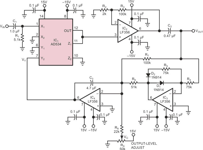
In the AGC circuit of Fig 1, a 4-quadrant analog multiplier (IC1), an amplifier stage (IC2), an active, full-wave rectifier (D1, D2, R4-R7, and IC3), and an integrator (IC4) accomplish automatic gain control of VIN’s amplitude variations in the audio-frequency range.
 |
|
| Figure 1. | Analog multiplier IC1 combines VIN with a feedback signal VY to achieve automatic gain control. |
The multiplier’s output is –V|NVY/10, where VY is a negative voltage generated by the integrator IC4. Together, the integrator and the rectifier extract the dc component (VY) of VOUT for use as a feedback signal to the multiplier. The integrator sums signal current from the rectifier and control current from potentiometer R9, which lets you adjust VOUT’s signal level.
Circuit analysis yields the frequency-response equation
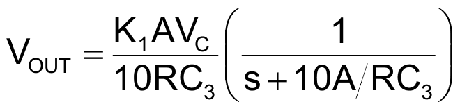
or, in the time domain,
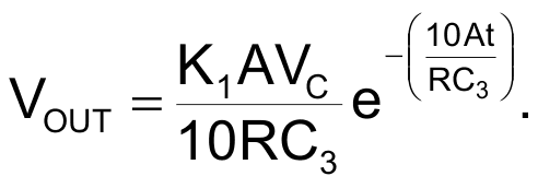
In both equations, K1 is the gain of amplifier IC2, A is the peak amplitude of VIN, and R is the resistance between the integrator input and the rectifier output. (For this circuit, R equals R6 in parallel with R7.)
This AGC circuit is suitable for controlling the long-term variations of amplitude within a limited range. It doesn’t respond uniformly over a wide dynamic range, however, because the time response is inversely proportional to input-signal amplitude.