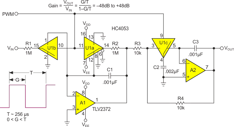
Pulse width modulation (PWM) is a simple and inexpensive (therefore popular!) way to implement moderate performance (e.g., 8 bit resolution low speed) digital to analog conversion, but improvising cheap DACs isn’t the only thing PWM can do. For example, Figure 1’s circuit illustrates using PWM to digitally set the analog gain of a versatile, robust, high (1 MΩ) input impedance, buffered output, DC input stage over a ~16 bit = 65280:1 = –48 dB to +48 dB attenuation/gain range.
 |
|
| Figure 1. | A PWM controlled amplifier/attenuator DC input stage. |
Here’s how it works: A 1 MHz, 8 bit (T = 256 µs period) PWM control signal runs three synchronous HC4053 SPDT CMOS switches designated U1a, U1b, and U1c. Its duty cycle = G/T = 0.4% to 99.6% as G = 1 to 255 µs.
U1b acts as a programmable input attenuator by steering the
input current alternately to ground or op-amp A1’s summing point, creating an input scale factor of
that’s programmable between near zero,
(G = 1 µs), to near unity
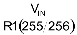
(G = 255 µs). Additionally, because of the near-zero summing-point-potential maintained at U1 pin15 by current steering, the accommodated VIN voltage range is very wide – limited mostly by R1’s axial voltage withstand capability which is typically 200 V for a ¼ W axial lead 1 MΩ resistor. Simultaneously, the millivolt range signal levels maintained across U1b’s switch elements (several orders of magnitude less than datasheet test conditions) reduce switch related leakage currents to << 1 nA; thus, minimizing leakage-related offset voltages to negligible levels despite the megohm R1.
Meanwhile, U1a is working to selectively steer current feedback from A1’s output to its summing point via R2 with a programmable factor of (1 – G/T), yielding a net V/I gain of
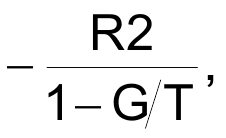
while maintaining similar leakage-minimizing millivolt voltage differentials across U1a’s switches.
The net effect makes A1’s voltage
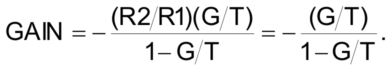
As G varies from 1 µs to 255 µs, there’s the stated
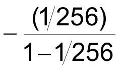
to
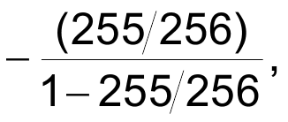
= –1/255 to –256 = 96 dB gain range, but what about that pesky minus sign and infamous PWM ripple?
Both signal inversion and ripple-suppression are performed by the sample and hold function implemented by U1c and A2, yielding a final ripple-free:
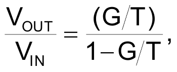
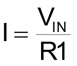
as graphed linearly in Figure 2 and logarithmically in Figure 3.
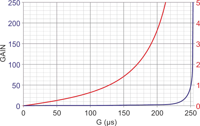 |
|
| Figure 2. | The linear gain plot (Red = 0 to 5 and Blue = 0 to 255). |
The positive (VDD) and negative (VEE) power rails are non-critical and noise-insensitive but ideally should be at least roughly symmetrical and will typically be +5 V and –5 V, respectively. Total current draw is less than 2 mA. Both C1 and C3 should be low-leakage types, polystyrene is suggested. Response time to an input or gain set step is somewhat gain dependent but is typically ~2 ms. Note that the R1C1 time constant is ~4T = 1 ms. Neither is exactly what you’d call lightning fast, but we are after all talking about PWM!
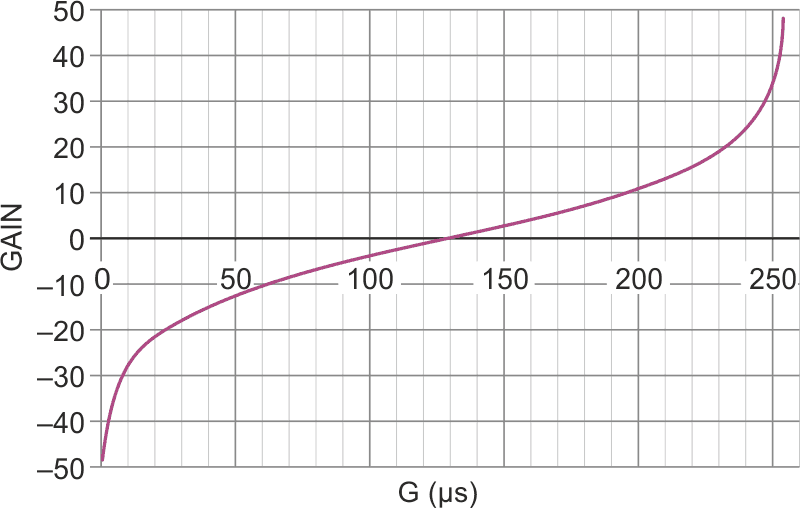 |
|
| Figure 3. | The log gain plot. |