Designers often use chargers with flyback topologies to quickly charge energy-storage capacitors (references 1 and 2). In a flyback topology, the energy transfer takes place only when the charger’s power MOSFET is off, which effectively isolates the power switch from the load, comprising high-energy storage-capacitor banks. Thus, the voltage levels on the circuit transformer’s secondary can vary from zero to a predetermined value and corresponding energy level without any significant stress on the components on the primary side of the transformer.
The classical flyback capacitor charger operates in CCM (continuous-conduction mode). Flat-topped, short-duration current pulses on the transformer’s secondary charge the storage capacitors (Reference 3). Unfortunately, this charging strategy requires complex control circuitry to limit both the secondary current and the capacitor voltage. Most circuits use a specialized PWM (pulse-width-modulation)-controller IC, which increases the overall cost of the charger. Another disadvantage of the CCM is the small portion of energy that accumulates during the on-time of MOSFET conduction:
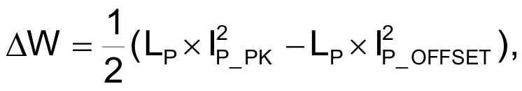
where IP_OFFSET signifies the initial nonzero primary current at the beginning of the on-time interval.
Only this limited portion of energy transfers from the primary to the secondary sides and enters the storage capacitor. Therefore, you can considerably increase the amount of energy transferable to the capacitive load if the converter can operate in BCM (boundary-conduction mode). The secondary current becomes zero, the power MOSFET turns on, and the primary current builds from zero. Thus, a bigger portion of energy accumulates during every consecutive on-time interval:
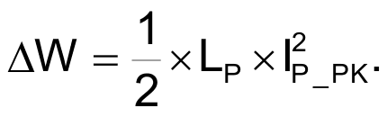
With all other conditions equal, BCM operation ensures faster accumulation of a predetermined amount of energy because of the bigger stored portions of energy during the on-time intervals. Many converter circuits that operate using BCM incorporate PWM controllers that implement BCM operation for capacitor charging. These circuits often use MAX8622 or LT3468 ICs. These ICs are specialized devices to accommodate BCM operation.
You can, however, implement flyback BCM operation without these specialized parts. Manufacturers implement BCM in the variable-frequency versions of flyback converters, which are quasiresonant, ZVS (zero-voltage-switching) converters that commonly find use in TV SMPS (switched-mode-power supplies). For example, you can use the STMicroelectronics quasiresonant-SMPS-controller L6565 to build a flyback capacitor charger working in BCM. Doing so eliminates the need for using a specialized chip for capacitor chargers.
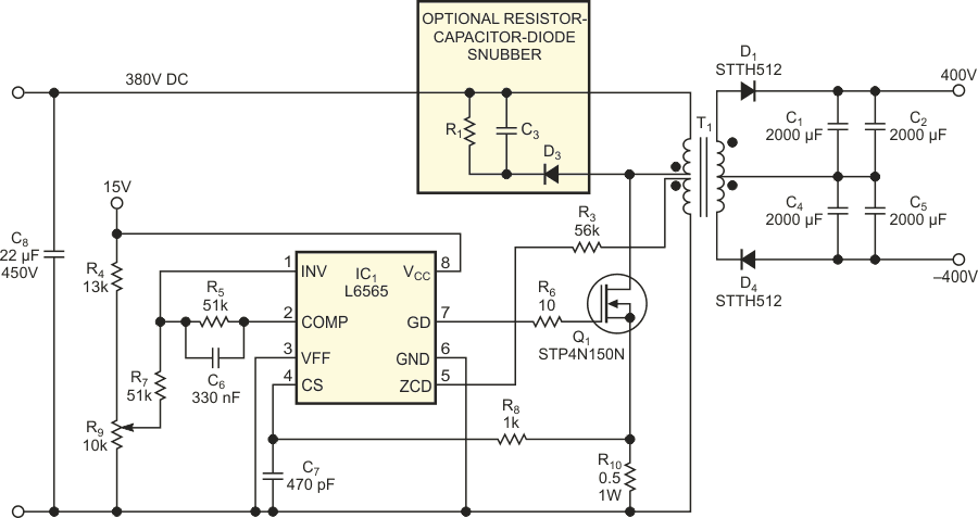
Figure 1 shows the power stage of a charger using the ST L6565. It achieves the BCM using a second primary winding on T1 that feeds the transformer-sensing input at the ZCD pin of the L6565. The voltage of this winding is a scaled-down replica of the drain-to-source voltage of power MOSFET Q1. When the circuit interrupts the secondary current – indicating full demagnetization of T1 – it detects the minimum of the first valley of ringing, and the L6565 turns on the MOSFET. This action eliminates the idling and zero-phase-time intervals, thus establishing BCM. The elimination of the zero-phase-time intervals greatly reduces the charging time of the storage capacitors.
 |
|
| Figure 1. | A flyback capacitor charger uses BCM operation. |
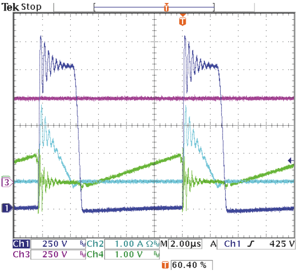
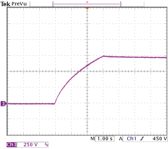
At the beginning of the charging sequence, the output voltage is low because of the large capacitance values. The secondary current decreases slowly. The reflected voltage on the primary side is too low to trigger the ZCD pin of the L6565. Thus, the L6565’s initial starting timer sets the switching frequency to 2.5 kHz at the start of charging. The output voltage across the storage capacitors increases to a point at which the switching frequency becomes variable because of the demagnetization of the transformer core. Figure 2 shows that, as soon as the secondary current (Channel 2) becomes 0 A, the power MOSFET turns on, and the drain-to-source voltage decreases (Channel 1). At that time, the primary current again increases (Channel 4). At the output voltage close to full charge, the switching frequency is approximately 100 kHz. Figure 3 shows the total voltage of 750 V across C1, C2, C4, and C5 within a 3-second charging time.
 |
|
| Figure 2. | When the secondary current reaches 0 A, the MOSFET turns on, and the primary current increases from 0 A. |
 |
|
| Figure 3. | The output-capacitor voltage reaches its full level in about 3 seconds. |
The waveforms in figures 2 and 3 are evaluation measurements of a prototype capacitive charger using the L6565 and power MOSFET STP4N150. A low-power PFC (power-factor-correction) stage, using transition-mode-PFC controller L6562, delivers the input-bus voltage of 380 V dc. This configuration ensures not only the dc-voltage bus for the power stage of the charger, but also a high power factor during the charging phase.
References
- Lan, Rayleigh, and Hunter Chen, “Flyback Charge Xenon Flash Capacitors.”
- Creel, Kirby, “Expedite Transformer Calculations for Flybacks.”
- N.O. Sokal and R. Redl, "Control algorithms and circuit designs for optimally flyback-charging of an energy storage capacitor (e.g., for flash lamp or defibrillator)."