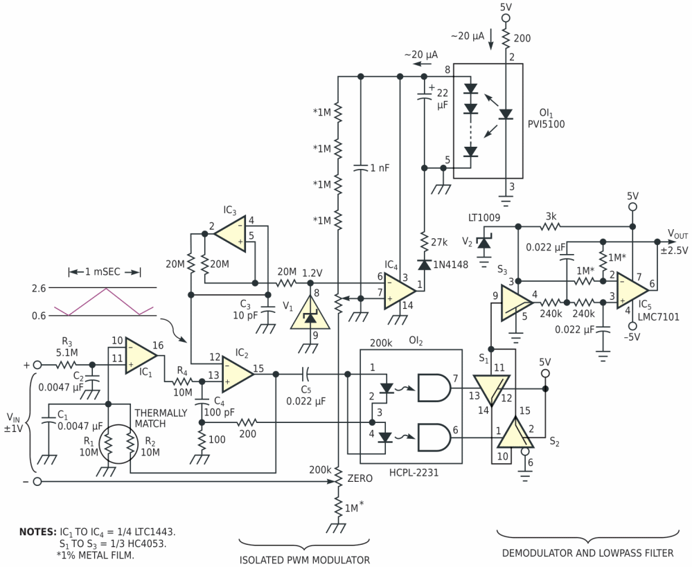
Self-powered isolation amplifiers, which need no external isolated power supply, provide versatile and convenient interfaces in many applications that require galvanic isolation of the signal source. Examples of such applications include circuits that serve in industrial or medical environments, in which isolation is necessary for noise reduction or safety. You can use a variety of isolated signal-coupling techniques for the signal paths of these amplifiers. Transformers, differential-capacitor, and optoisolator schemes are all popular choices. For the internal isolated power supply, transformer coupling is virtually universal, despite the problems inherent in inductively coupled circuits. These problems include relatively high interwinding stray capacitance and a tendency to couple switching noise into the signal. In contrast, the self-powered amplifier in Figure 1 is different in that it incorporates optoisolators to effect communication of both signal and power around the isolation barrier.
 |
|
| Figure 1. | A virtual perpetual-motion machine (when there’s light), this self-powered amplifier provides complete galvanic isolation for both power and signal. |
As in many isolation-amplifier designs, the signal processing in Figure 1’s circuit uses PWM. The isolated-modulator front-end circuitry derives from an earlier ADC design and works as follows. IC1 compares the ±1 V filtered input signal with the voltage on C1. The R4C4 time constant smoothes IC1’s output, and IC2 compares the output with IC3’s approximately 1-kHz triangle waveform. R1, R2, and C1 scale and average the resulting variable-duty-factor square wave and feed the signal back to IC1. This feedback loop continuously adjusts IC2’s duty factor to maintain equal voltages on C1 and C2. In doing so, the feedback forces IC2’s output square wave to track the unique T+/(T+ + T–) duty factor that maintains balance at IC1’s inputs.
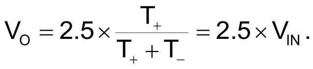
C5 differentiates the IC2 square wave to provide bipolar drive pulses to the antiparallel LEDs in the high-speed, low-current optoisolator OI2. In turn, OI2 produces ground-referred pulses. The rather unusual RS flip-flop formed by cross-connected switches S1 and S2 converts these pulses back to a logic-level square wave having the same duty factor as IC2’s output. Demodulation and filtering of the square wave to accurately reproduce the original analog signal occurs through the action of the single-pole, double-throw switch, S3, which chops the 2.500 V V2 reference voltage according to the T+/(T+ + T–) square-wave duty factor. The low-pass, gain-of-two filter, IC5, then extracts the dc component of S3’s 0 to 2.5 V waveform and scales and offsets it to produce a low-ripple, ±2.5 V signal, according to the formula
Power for the isolated-modulator side of the amplifier comes from OI1, a PVI5100 photovoltaic opto IC. Marketed as an isolated MOSFET-gate driver, the PVI5100 can source approximately 20 mA of current at 4 V (80 mW), just enough to keep the anorexic LTC1443 alive and functional. IC4 shunt-regulates OI1’s output to provide a stable 4 V ratioed against the LTC1443’s 1.2 V±1% internal reference. Overall frequency response is dc to 10 kHz; input impedance is approximately 1 TΩ with less than 1-pA bias. The circuit can thus provide good overall accuracy with high-impedance input sources. You can trim gain and offset errors to zero; the excellent drift specs of the LTC1443 maintain the trim over temperature.
Materials on the topic
- Datasheet Microchip LMC7101
- Datasheet Analog Devices LT1009
- Datasheet Linear Technology LTC1443
- Datasheet NXP 74HC4053
- Datasheet Avago Technologies HCPL-2231
- Datasheet International Rectifier PVI5100