An interesting variation on the theme of digital to analog converters (DACs) is the digital potentiometer (DPOT). In addition to being able to output a voltage proportional to a digital value when used as a multiplying DAC (MDAC), the DPOT can also work as a digitally programmed resistor (rheostat). When used this way, an important parameter that sometimes limits DPOT accuracy is wiper resistance: RW.
Of course, being solid state devices, unlike electromechanical potentiometers DPOTs don’t have a physical resistance element with an actual wiper running around on it. What their “RW” really comprises is the ON resistances of the array of FET switches that select the desired tap on the internal resistor ladder (26 + 1 = 65 taps for a 6 bit pot, 27 + 1 = 129 for 7 bits, 28 + 1 = 257 for 8, etc.). RW effectively appears in series with the selected resistance so that if:
RAB = total resistor ladder resistance = 5k (typical) for exemplar DPOT (MCP4161-502).
N = ladder tap selection setting (0 ≤ N ≤ 256 for 8 bit exemplar).
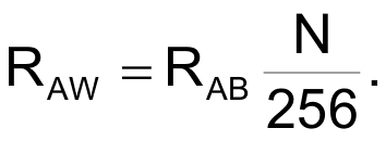
Then in an ideal world (where all RW = 0), the resulting resistance would be simply:
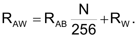
Unfortunately, in the world of real DPOTs, RW > 0. Consequently:
For the exemplar 8 bit 5k DPOT, RW = 75 ohms (typical, 160 max), setting a minimum (N = 0) RAB = 75/5000 × 256 = ~4 lsb (typical) 8 lsb (max).
Being unable to set RAB < 75 ohms for N = 0 may already be problematic for many applications, but the ill effects of RW > 0 extend to other N. For example, the RAB ladder tempco of the MCP41 series is an excellent 50 ppm/°C (typical), but RW’s tempco is orders of magnitude worse at ~3000 ppm/°C. Therefore, RW dominates net tempco for any N < 230.
Suffice to say, cancellation of RW would make worthwhile improvements to DPOT performance in many precision applications. Figure 1’s topology does this. Here’s how it works.
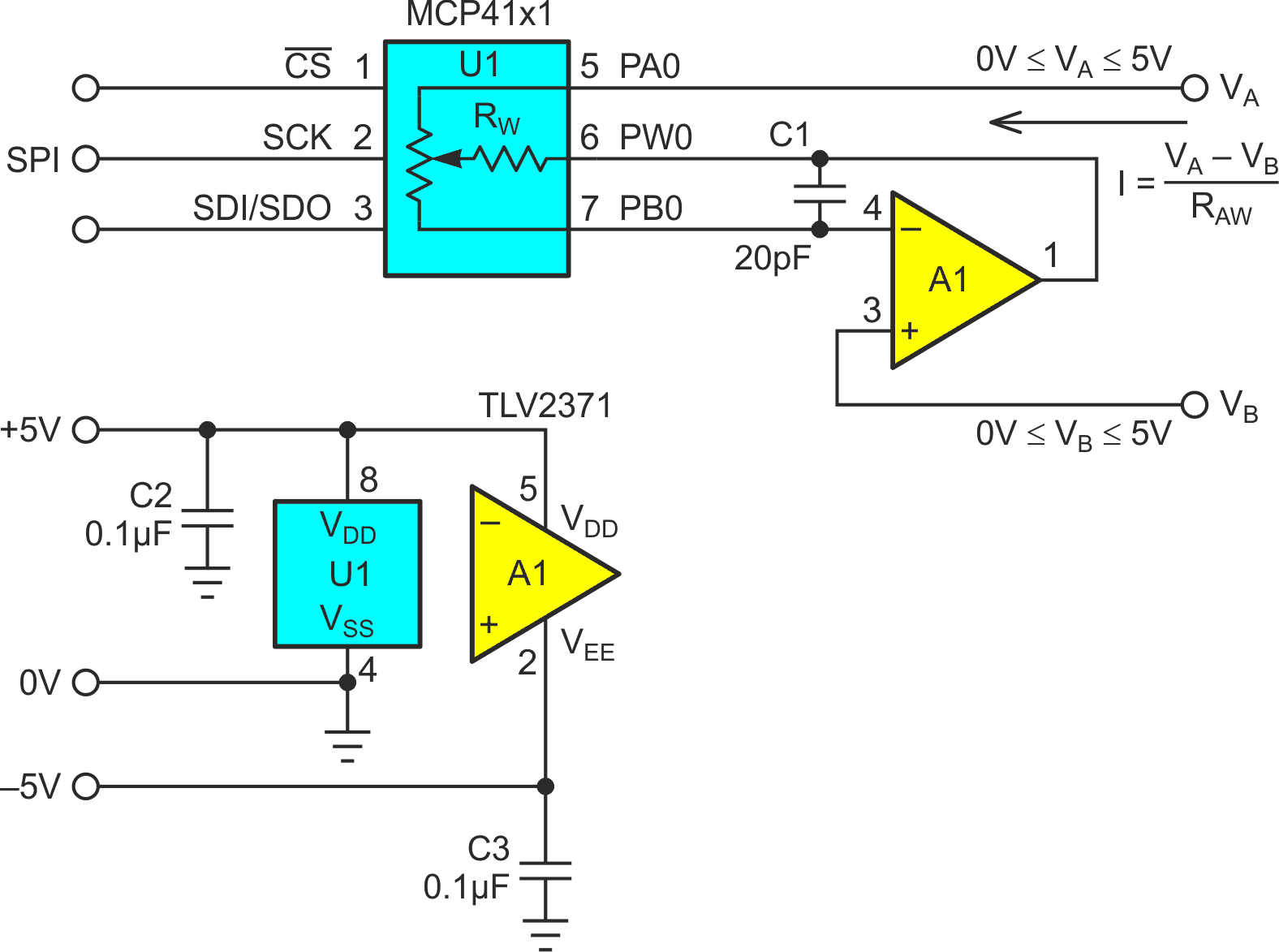 |
|
| Figure 1. | Op-amp A1 actively drives digital pot U1 wiper terminal PW0 to force VPBO = VB while drawing negligible current through resistance RWB, thus cancelling the effect of RW. |
The connections of A1’s (+) input to reference voltage VB (typically, but not necessarily, ground), (-) input to U1’s PB0 pin, and its output to U1’s PW0 pin establishes a feedback loop that forces VPBO = VB independently of RW. This, as advertized, wipes out RW effects.
Compensation capacitor C1 probably isn’t absolutely necessary for the part selection shown in Figure 1 for A1 and U1, but if a faster A1 amplifier or a higher RAB resistance DPOT where chosen, it probably would be.