This Design Idea significantly improves conversion efficiency of externally driven flyback converter-based capacitor charging units intended for flash-lamp-pumped, pulsed solid-state laser sources. In a flash-pumped pulsed solid state laser source, an energy storage capacitor is charged to a high voltage, dependant upon the amount of energy it is intended to deliver to the flash lamp when made to discharge.
Flyback converter topology suits capacitor charging power supply design well. Conventional flyback converter circuits employing voltage feedback for achieving the desired output voltage, and pulse width modulation for voltage regulation, cannot be used in the case of capacitive load due to the following reason:
In a flyback converter, energy is stored during the on-time of the switching device, and transferred during the off-time. A large number of storage and transfer cycles are needed to charge the energy storage capacitor to the desired value. For a given amount of stored energy, the transfer of energy in every single transfer charges the capacitor by a certain voltage step, the size of which keeps reducing as the voltage across the capacitor builds up. As a result, the desired off-time changes from an initial maximum to a minimum value in the last storage and transfer cycle that takes the load to its final voltage. Any attempt to design the converter using a fixed switching frequency results in poorer efficiency. In the case of higher switching frequency, energy transfer would be incomplete in the earlier charging phase. This may lead to damage of circuit components connected on primary side. There is also a chance of core saturation due to residual flux. In the case of lower switching frequency, the converter would be sitting idle for most of the time during the latter part of charging.
We have adopted a design approach based on a closed loop feedback system which ensures that energy transfer is complete in all individual cycles of the input waveform. In fact, the system is such that the status of the energy storage capacitor voltage is monitored at all times. Each cycle time period is reduced, keeping on-time fixed. That is, the off-time is reduced as per the requirement of the energy transfer process. So we have the ideal situation that ensures fastest possible charging time as well as optimum transformer design.
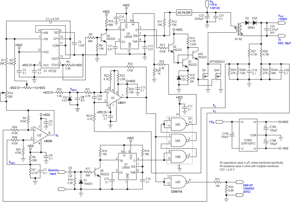
The circuit shown in Figure 1 is that of a flyback converter-based capacitor charging unit for a Q-switched Nd:YAG laser operating at 20 Hz. The design charges an energy storage capacitor (ESC) of 30 µF with the desired energy of 15 joules in less than 50 ms so as to ensure operation at 20 Hz.
 |
|
| Figure 1. | А flyback converter-based capacitor charging unit. |
The circuit operates in an externally driven flyback configuration. Energy is stored during the on-time of the switching MOSFET and transferred to the energy storage capacitor during the time when it is switched to off-state. Each time the energy is transferred to the secondary circuit, the output capacitor charges by a certain voltage step. The magnitude of this step decreases with the buildup of voltage across the capacitor. The reduction of off-time of the switching device follows the same pattern as the buildup of voltage across the capacitor. The voltage across the energy storage capacitor is sensed and a control voltage VS is generated. This voltage is fed to a subtractor U2 that subtracts a negative reference voltage VREF1 from the control voltage. The output of subtractor is VR = VS – VREF1, which is fed to voltage-to-frequency converter (VFC) U1; hence the operating frequency is changed linearly with the voltage across the capacitor.
Initially, when the ESC is uncharged, the output voltage is zero and VS = VS(MIN) = 0 V. At the output of U2, we have small positive voltage (VR(MIN) or –VREF1). This voltage determines the initial period at the VFC output. This output goes to monostable multivibrator U5 to achieve a fixed on-time. As the ESC voltage builds, the control voltage to the VFC converter increases, which reduces the off-time. A voltage sense loop compares VC – a fraction of the output voltage – with reference voltage VREF2 to generate the reset pulse for the monostable circuit and consequently achieve the desired output voltage.
The unit also has a feature of quenching the converter that prevents “afterglow” of the flash lamp. For quenching of the flash lamp, the charging of the ESC must be disabled for a few milliseconds at the instant of the flash lamp firing command. This is achieved by holding off U5 during this period. The holdoff is generated by triggering a second monostable, U7, by the firing command pulse. The EOC output indicates that the charging process has been completed.
Appendix. Transformer design
The transformer was designed to deliver an output power of 300 W (15 J of energy at 20 Hz rate), and a conversion efficiency of 80% was assumed.
| Core Type | EE 4215 (Make Cosmo Ferrite Limited) |
| Effective magnetic path length | 97 mm |
| Effective cross-sectional area | 181 mm2 |
| Maximum saturable flux density | 390 mT |
| Operating maximum flux density value taken for the design to avoid core saturation |
300 mT |
| Initial Permeability | 3,000 |
| Primary turns, NP | 11 |
| Secondary turns, NS | 275 |
| Primary Inductance, LP | 10 µH |
| Peak primary current, IP | 60 A |
| Constant ON-time of the switching MOSFET | 25 µs |