Junction field-effect transistors (JFETs) usually require some reverse bias voltage to be applied to a gate terminal.
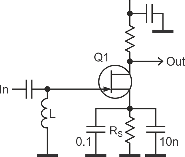
In HF and UHF applications, this bias is often provided using the voltage across the source resistor RS (Figure 1).
 |
|
| Figure 1. | JFETs typically require some reverse bias across the gate terminal and in HF/UHF applications, this is often provided using the voltage across resistor RS. |
Barring the evident lack of efficiency, such approach has other shortcomings as well:
- The drain current has statistical dispersion, so to get a target value of the current some circuit adjustment is required.
- The drain current may depend on temperature or power fluctuations.
- To achieve an acceptable low source impedance, several capacitors CS have to be used.
- To maintain the same headroom a higher power voltage is required.
- The lack of direct contact with the ground plane means worse cooling of the transistor, which is crucial for power applications.
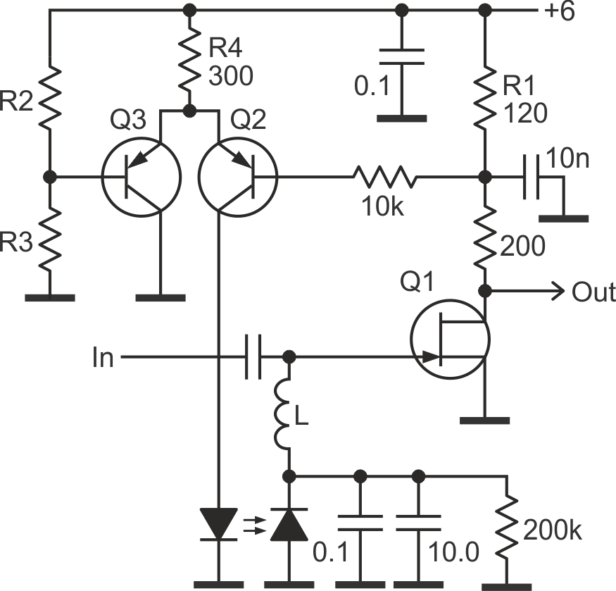
The circuit in Figure 2 is free of all these. It consists of a control loop which produces control voltage of negative polarity for n-channel JFET amplifier.
 |
|
| Figure 2. | A control loop that produces control voltage of negative polarity for n-channel JFET amplifier in HF and UHF applications. |
The circuit uses two infrared LEDs IR333C (diameter = 5 mm) in a self-made photocoupler. Two such LEDs placed face-to-face in an appropriate PVC tube about 12 mm long, that’s all. One such device produces 0.81 V @ ILED < 4 mA, which is quite sufficient for the HEMT FHX35LG, for example.
Of course, if you need higher voltage, several such devices can be simply cascaded.
The main amplification in the loop is performed by the JFET itself. Its value is about gm×R1, where gm is a transconductance of Q1.
The transistor pair Q2 and Q3 compares the voltage drops on the resistors R1 and R2 making them equal. Hence, by changing the ratio R2:R3 you can set the working point you need:
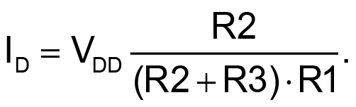
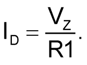
As we can see, the drain current (ID) still depends on power voltage (VDD). To avoid this dependence, we can replace resistor R2 with a Zener diode, then: