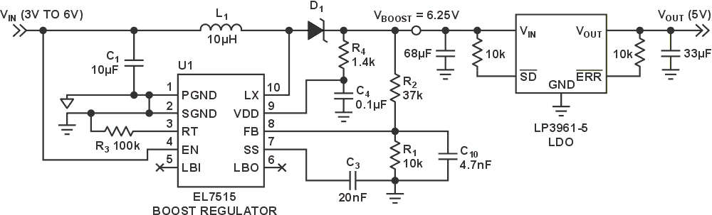
A stable voltage from an input supply that is higher and lower than the output is often required. A common solution is to use a boost converter followed by an LDO as shown in Figure 1. The boost converter is configured to accept voltages ranging from 3 V-6 V and to produce an output of 6.25 V. The 6.25 V is then regulated to 5 V by the LDO. Both stages of this solution exhibit some conversion losses. A simpler, one-stage solution with a boost converter offers higher efficiency. This simple solution with a PFET transistor is presented in detail and compared to the common solution.
 |
|
| Figure 1. | Typical 5 V regulation with boost converter and LDO. |
When using a boost converter, the output has to be set above the highest input voltage to avoid significant losses. Therefore, the output of the boost converter in Figure 1 has been set to 6.25 V. A low drop-out voltage regulator is then used to acquire the desired final voltage of 5 V. The efficiency of this set-up can be calculated from the efficiency of each of the components by this formula:

The efficiency of the boost converter ηBOOST is typically 90%; however, the efficiency of the LDO ηLDO is ratio of the output and input (5 V/6.25 V), 77%. The overall efficiency is 69%. That difference is a trade-off among the voltage needed at the output of the boost converter, the drop-out voltage of the LDO, and margin for the system.
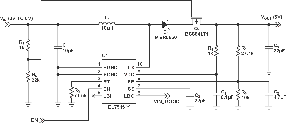
To achieve a sizable increase in the efficiency of this system, a single-stage solution is needed. A single-stage boost circuit is given in Figure 2. The Schottky diode in series with the PFET keeps the output of the regulator at a voltage greater than the system output voltage – keeping the boost converter in its high-efficiency operating mode. The voltage value at the output of the boost converter is set by the combination of the turn-on voltage of the PFET and the result of the voltage divider attached to its gate.
 |
|
| Figure 2. | 5 V regulation with boost converter and FET. |
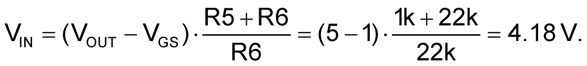
The PFET acts like a linear resistor with 1.0 V VGS threshold. It is fully on when the input is below 4.2 V. When the input is greater than 4.2 V, pin 10 of the boost converter needs to rise above the input voltage. Therefore, the voltage divider of R5 and R6 begins to turn the transistor off to increase channel resistance. This inserted resistance further isolates the output of the boost regulator from the output of the system and adds the voltage drop of the channel resistance, allowing the boost regulator to remain efficient and stable. The combination of PFET VGS threshold and the R5 and R6 resistor divider ratio determines the input voltage level that PFET is turned fully on.
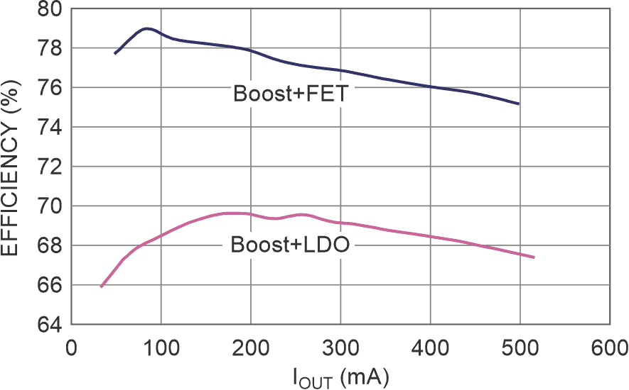
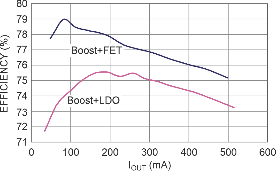
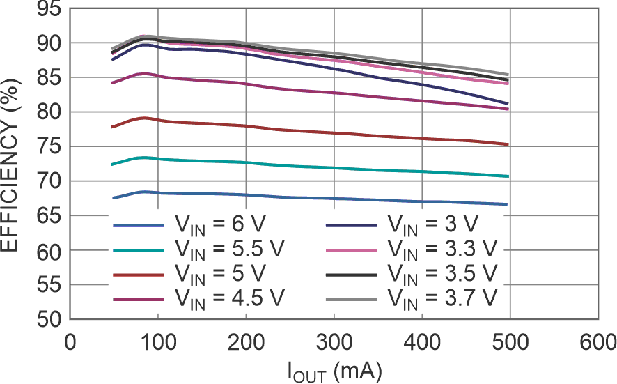
A comparison of the efficiency of each system is presented in Figure 3. With a low voltage input (3.3 V) being converted to 5 V, the boost converter with PFET consistently provides 8% higher efficiency over the boost/LDO combo shown in Figure 1. With the circuits under greater stress (as with VIN = 5 V), the boost/FET circuit remains more efficient, about +4% at low current and +2% for high current uses (Figure 4).
 |
|
| Figure 3. | Efficiency of boost/LDO combo and boost/FET combo for VIN = 3.3 V, VOUT = 5 V. |
 |
|
| Figure 4. | Efficiency of boost/LDO combo and boost/FET combo for VIN = 5 V, VOUT = 5 V. |
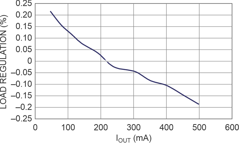
To examine the efficiency for the spectrum of input voltages, Figure 5 is provided. The efficiency of the system is well above 80% for input voltages less than or equal to the output voltage. When the input voltage is increased, the efficiency drops by about 1% per 100 mV. A load regulation curve (Figure 6) is included to show the precision of the output voltage versus current.
 |
|
| Figure 5. | Efficiency of boost/FET combo for VOUT = 5 V, VIN varied. |
 |
|
| Figure 6. | Load regulation of boost/FET combo. |