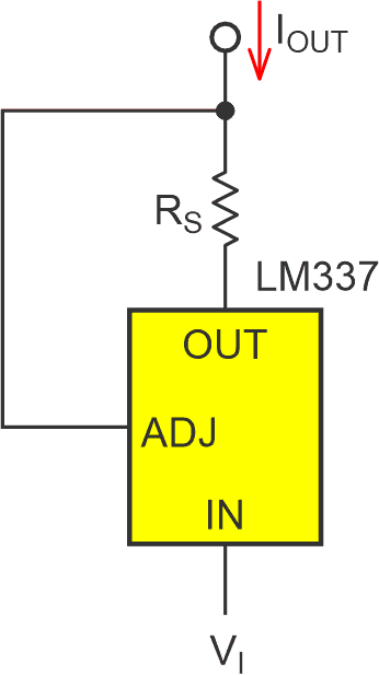
Figure 1’s negative constant current source has been a textbook application for the LM337 regulator forever (or thereabouts). It precisely maintains a constant output current (IOUT) by forcing the OUTPUT pin to be the negative VADJ relative to the ADJ pin. Thus, IOUT = VADJ/RS.
 |
|
| Figure 1. | Classic LM337 constant negative current source where IOUT ≈ VADJ/RS = 1.25/RS. |
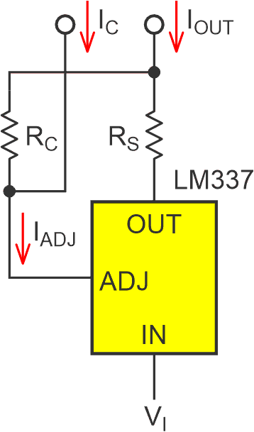
It has worked well for half a century despite its inflexibility. I say it’s inflexible because the way you program IOUT is by changing RS. It may be hard to believe that a part so mature (okay old) as the 337 might have any new tricks left to learn, but Figure 2 teaches it one anyway. It’s a novel topology with better agility. It leaves the resistors constant and instead programs IOUT with the (much smaller) control current (IC).
 |
|
| Figure 2. | RC typically >100RS, therefore IC < IOUT/100 and IOUT ≈ –(1.25 – (ICRC))/RS. |
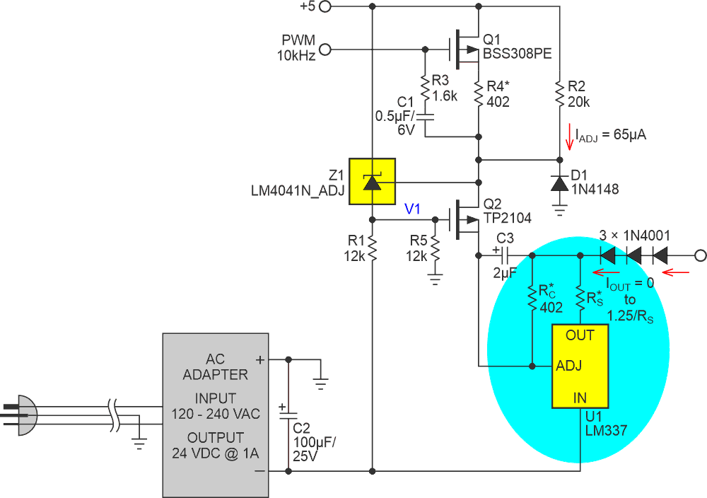
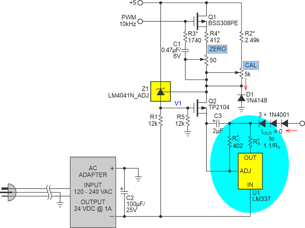
RC > 100RS allows control of current of IOUT with only milliamps of IC. Figure 3 shows the idea fleshed out into a complete PWM-controlled 18 V, 1 A grounded-load negative current source.
 |
|
| Figure 3. | An 18 V, 1 A, PWM-programmed grounded load negative current source with a novel LM337 topology. With this topology, accuracy is insensitive to supply rail tolerance. The asterisked resistors are 1% or better and RS = 1.25 Ω. |
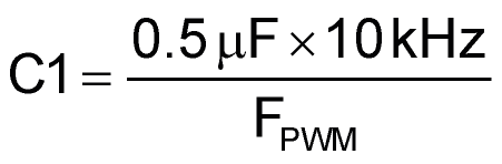
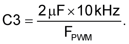
The PWM frequency, FPWM, is assumed to be 10 kHz or thereabouts, if it isn’t, scale C1 and C3 appropriately with:
and,
The resulting 5-Vpp PWM switching by Q1 creates a variable resistance averaged by C1 to R4/D, where D = the 0 to 1 PWM duty factor. Thus, at Z1’s Adj point:
The second-order PWM ripple filtering gives a respectable 8-bit settling time of 6 ms with FPWM = 10 kHz.
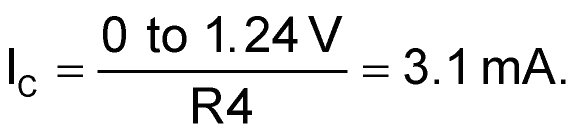
Z1 servos the V1 gate drive of Q2 to hold the FET’s source at its precision 1.24-V reference and then level shift the resulting IC to track U1’s ADJ pin. Also summed with IC is IADJ bias compensation (1.24 V/20k = 62 µA) provided by R2.
This term zeros out U1’s typical IADJ and cuts its max 100 µA error by 60%. Meanwhile, D1 insures that IOUT is forced to zero when 5 V drops by saturating Q2 and making IC large enough to turn U1 completely off, thus protecting the load.
About the 1N4001 daisy chain: There’s a possibility of IOUT > 0 at IC = max and a resulting reverse bias of the load; some loads might not tolerate this. The 1N4001s block that, and also provide bias for the power-down cutoff of IOUT when +5-V rail shuts down.
Note that the accuracy of ICRC = VADJ is assured by the match of the RC resistors and precision of the Z1 and U1 internal references. It’s therefore independent of the tolerance of the +5-V rail, although it should be accurate to ±5% for best PWM ripple suppression. IOUT is linear with PWM duty factor D = 0 to 1:
If RS = 1.25 Ω, then IOUT(MAX) = 1 A.
Note that U1 may have to dissipate as much as 23 W if IOUT(MAX) = 1 A and the load voltage is low. Moral of the story: Be generous with the heatsink area! Also, RS should be rated for a wattage of 1.252/RS.
Figure 4 shows modifications to facilitate wiping out component tolerances including those of U1 and Z1 references and all resistors.
 |
|
| Figure 4. | Modifications to facilitate wiping out component tolerances including those of U1 and Z1 references and all resistors. Note that RS = 1.1 ohm. |
The one pass calibration sequence is:
- Set D = 100%
- Adjust CAL pot for 1.000 amp output current
- Set D = 0%
- Adjust ZERO pot for zero output current.
Done. IOUT = 1.1 D/RS.