The LM4041 has been around for over 20 years. During those decades, while primarily marketed as a precision adjustable shunt regulator, this classic device also found its way into alternative applications. These include voltage comparators, overvoltage protectors, voltage limiters, etc. Voltage, voltage, voltage, must it always be voltage? It gets tedious. Surely this popular precision chip, while admittedly rather – um – “mature”, must have untapped potential for doing something that doesn’t start with voltage.
The Design Idea (DI) presented in Figure 1 offers the 4041 a usual, possibly weird, maybe even new role to play. It’s a precision current source.
 |
|
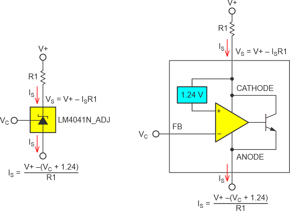
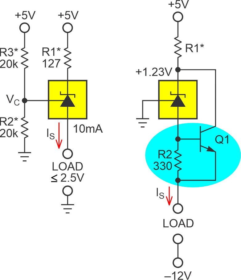
| Figure 1. | Weirdly, the “CATHODE” serves as the sense pin for active current source regulation. |
The above block diagram shows how the 4041 works at a conceptual level:
Sourced current =
IS > 0, V+ < 15 V, IS < 20 mA.
The series connection subtracts an internal 1.24-V precision reference from the external voltage input on the CATHODE pin. The internal op-amp subtracts the voltage input on the FB pin from that difference, then amplifies and applies the result to the pass transistor. If it’s positive [(V+ – 1.24) > VC], the transistor turns on and shunts current from CATHODE to ANODE. Otherwise, it turns off.
When a 4041 is connected in the traditional fashion (FB connected to CATHODE and ANODE grounded), the scheme works like a shunt voltage regulator should, forcing CATHODE to the internal 1.24-V reference voltage. But what will happen if the FB pin is connected to a constant control voltage [VC < (V+ – 1.24 V)] and CATHODE – and instead of being connected to FB – floats freely on current sensing resistor R1?
What happens is the current gets regulated instead of the voltage. Because VC is fixed and can’t be pulled up to make FB = CATHODE – 1.24, CATHODE must be pulled down until equality is achieved. For this to happen, a programmed current, IS, must be passed that is given by:
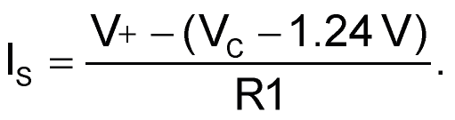
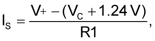
Figure 2 illustrates how this relationship can be used (assuming a 5-V rail that’s accurate enough) to make a floated-cathode 4041 regulate a constant current source of:
It also illustrates how adding a booster transistor Q1 can accommodate applications needing current or power beyond Z1’s modest limits. Notice that Z1’s accuracy will be unimpaired because, with whatever fraction of IS that Q1 causes to bypass, Z1 is summed back in before passing through R1.
 |
|
| Figure 2. | The booster transistor Q1 can handle current beyond 4041 max IS and dissipation limits. |
Figure 3 shows how IS can be digitally linearly programmed with PWM.
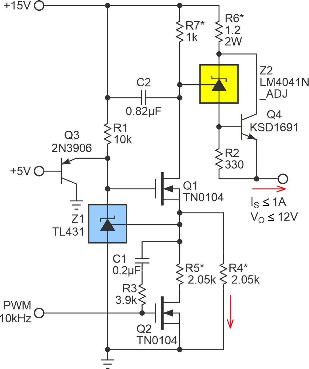 |
|
| Figure 3. | Schematic showing the DAC control of IS. IS = D amps, where D = PWM duty factor. The asterisked resistors should be 1% or better. |
Incoming 5-Vpp, 10-kHz PWM causes Q2 to switch R5, creating a variable average resistance = R5/D. Thanks to the 2.5-V Z1 reference, the result is a 0 to 1.22 mA current into Q1’s source. This is summed with a constant 1.22 mA bias from R4 and level shifted by Q1 to make a 1.22 to 2.44 V control voltage, VC, for current source Z2.
The result is a linear 0- to 1-A output current, IS, into a grounded load where IS = D amps. Voltage compliance is 0 to 12 V. The 8-bit compatible PWM ripple filtering is 2nd order using “Cancel PWM DAC ripple with analog subtraction” (Ref. 1)
R3C1 provides the first-stage ripple filter and R7C2 the second. The C1 and C2 values shown are scaled for FPWM = 10 kHz to provide an 8-bit settling time of 6 ms. If a different PWM frequency is used, scale both capacitors by 10 kHz/FPWM.
A hot topic is that Q4 can be called on to dissipate more than 10 W, so don’t skimp on heatsink capacity.
Q3 is a safety shutdown feature. It removes Q1 gate drive when +5 falls below about 3 V, shutting off the current source and protecting the load when controller logic is powered down.
 |
|
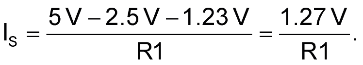
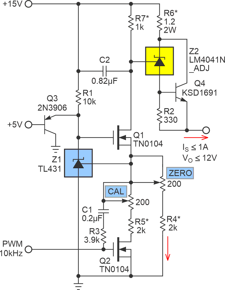
| Figure 4. | Additional zero and span pots to implement a single-pass calibration for best accuracy. |
Figure 4 adds zero and span pots to implement a single-pass calibration for best accuracy:
- Set D = 0% and adjust single turn ZERO trim for zero output current
- Set D = 100% and adjust single turn CAL trim for 1.0 A output
- Done.
Reference
- Woodward, Stephen. "Cancel PWM DAC ripple with analog subtraction."