Introduction
These ultra-simple projects are intended to provide two simple functions without the need for transformers or 'esoteric' parts. The first is a simple charge-pump voltage booster, that will raise your supply voltage by a factor of two - at least in theory. Reality is different, because there are losses in the 555 timer and in the Schottky diodes.
The latter can be minimised by using higher current diodes, but there's still a small loss.
 |
|
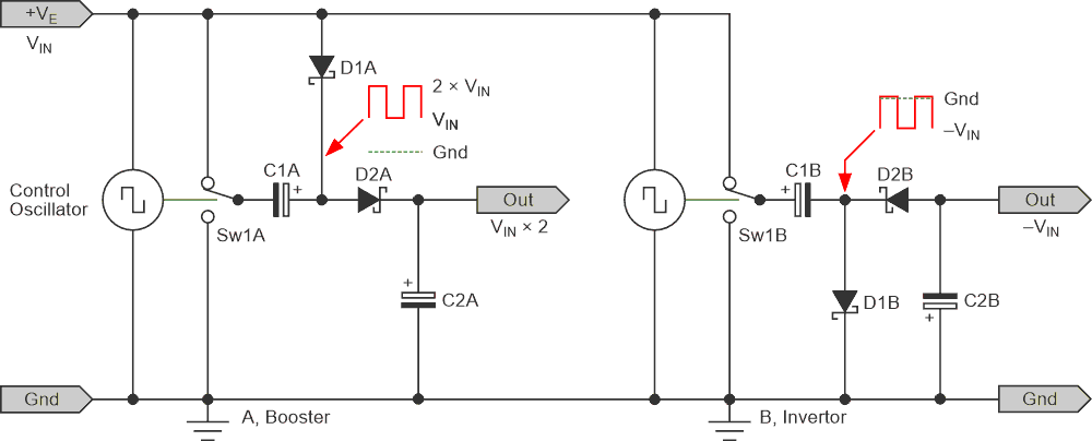
| Figure 1. | Boost (A) and invert (B) circuit operating principles. |
The second circuit generates a negative voltage, often useful or essential for a project where only a single supply is available. The negative voltage is a little lower than the positive supply, again because of losses in the timer IC and Schottky diodes. These losses are inevitable, and while it is possible to reduce them, it adds complexity to what is meant to be a simple circuit. Dedicated ICs can have surprisingly complex internal circuits, and it would not be sensible to try to reproduce these in discrete circuitry.
Neither circuit is designed for high current, and this type of circuit is most often used when you need a higher (or negative) voltage, but only at a few milliamps. Mostly, this type of circuit (at least when using a 555 timer IC) is used where you only need up to 20 mA. You can get more, but the voltage will sag rather badly above 30 mA or so. In many cases this won't matter. If your expected current is very low (< 5 mA) you may be able to use the 7555 – the CMOS version of the 555 timer. It can operate faster (up to 500 kHz), but can't supply much current, and that is its main limitation. Mostly you'll use a 'standard' 555 timer which can supply more current (source and sink).
The circuits are shown with an assumed 12 V supply, but they will work with 9 V (with additional losses) or up to 15 V, the maximum recommended for the 555 timer IC. Operation at 5 V is theoretically possible, but the performance will be very poor. Both can be used to 'stack' a power supply, so you could get a +47 V supply 'stacked' on top of a +35 V supply. The same is possible for the negative voltage generator, but great care is needed to ensure that the output pin of the 555 timer can never be forced below zero (that can cause the IC to latch, and it requires a power off-on sequence to re-start).
Project description
The principle of a charge-pump is pretty straightforward. A switching system connects the output alternately between the positive supply and ground, ideally with no voltage drops due to transistors or series resistance. Since ICs all use transistor switches, there are inevitable losses. Dedicated charge-pump ICs minimise these losses, but they can't be eliminated. The operation of a booster is quite different from that for a voltage inverter, but they tend to be lumped together in most descriptions. Despite initial appearances, the voltage across C1 (either circuit) barely changes once the initial set-up conditions are established. There is ripple current though, and it's roughly twice the output current.
The 'ideal' switches are toggled by the control oscillator, and when one contact is open the other is closed. We'll look at the boost circuit first (Figure 1, left). When the switch is closed to ground, C1A charges via D1A from the supply to ground. When the switch changes state, the charge on C1A boosts the positive end to twice the input voltage (2 × VIN). This doubled voltage is transferred to C2A via D2A. If there were no voltage drops across the diodes, the output voltage would be exactly double the input (DC) voltage. The output cap (C2A) must have a voltage rating to suit the maximum output. It's also possible to connect the negative of C2A to +VE – it's rarely seen, but works perfectly well, and means the cap's voltage rating doesn't need to be 2 × +VE.
The negative voltage generator circuit works very differently (Figure 1, right). The connection of C1B and D1B forms a simple voltage clamp, with the input voltage varying from zero to +VE. Back in the days of analogue television, this circuit was commonly known as a 'DC restorer'. When the switch is connected to +VE, C1B charges via D1B. When the switch connects to ground, the positive of C1B is grounded, so the negative terminal has –VE on it, which is coupled to C2B via D2B so C2B now also has –VE across it. This is the negative supply. The rectifier is half-wave. C2B is charged at the switching frequency.
The output ripple is determined by the switching speed, the value of C1 and C2, and the load current (Figure 2). In general, C1 and C2 are usually made equal, but it's often quite aright if C1 is a lower value. For example, C1 might be 33 μF, while C2 could be 100 μF. If they aren't equal the output voltage is reduced a little, and ripple is increased. 100 μF is a good 'general purpose' value, but if the required current is less than 10 mA, the caps can be reduced. I don't recommend anything less than 33 μF though, because the 555 timer doesn't like high frequencies. Operation at (or around) 30 kHz is a reasonable compromise.
 |
|
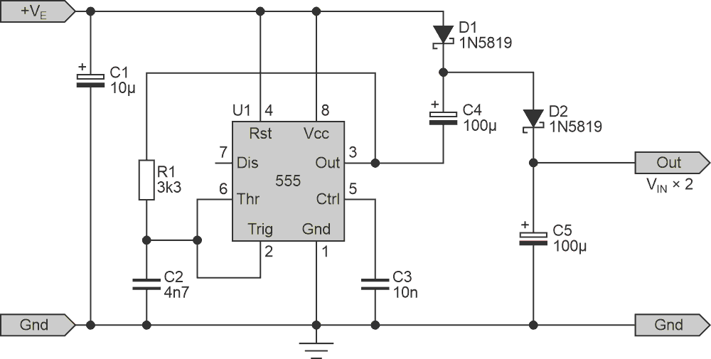
| Figure 2. | Boost circuit: 12 V in, 24 V out (nominal). |
With the 'ideal' circuits shown above, the output ripple is about 5.4 mV p-p for the doubler (100 μF, 30 kHz) and 4.7 mV p-p for the inverter (same values). This is with an output current of (very roughly) 10 mA for both. If the capacitance is increased by a factor of three, the ripple is reduced by the same amount. Likewise, if the oscillator frequency is halved, the ripple is doubled.
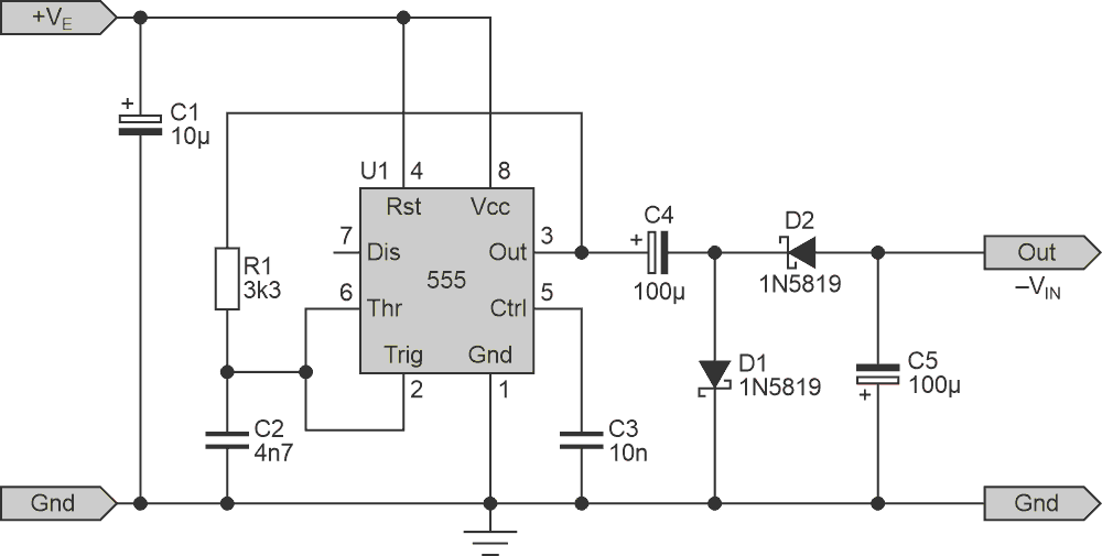
Neither circuit is designed for high current, and in general it should be no more than 10 mA or so. The 555 timer is configured as a 'minimal component count' oscillator, saving a resistor compared to the 'conventional' astable (no stable state) oscillator. The frequency is nominally about 32 kHz to ensure that it's out of hearing range. You can get around 20 mA if you're willing to lose 4 V (12 V in, –12 V out or 12 V in, 24 V out). The actual outputs will be around –8 V or +20 V (inverting, boosting respectively).
I've kept the circuit as simple as possible. Using Schottky diodes is a must if you're struggling for the last bit of voltage, but otherwise you can use 1N4148 diodes. These circuits are deigned for low current, and while a higher current version is possible, it becomes irksome. There are dedicated ICs that perform the same task with fewer external parts, but some are surprisingly expensive for something that's really quite pedestrian. The TC7660(S) (negative voltage converter) is low cost (under AU$2.00 each) but they are dedicated to negative conversion mode. They also have a limited supply voltage (10 V for the 7660, 12 V for the 7660S). Like most of these ICs, they are not designed for high current. Many are in SMD packages, with some using the least user-friendly packages possible (leadless chip carriers – LLCC) which is most unhelpful for DIY projects.
The inverting circuit in Figure 3 (if 100% efficient) would provide a –12 V supply. The limitation is the 555 itself, as it can't source or sink enough current to get the full 0-12 V output swing under load. The maximum is around 10 V, with a minimum of 750 mV (at an output current of +26 mA and –36 mA). The diodes also reduce the available voltage, because even Schottky diodes have a forward voltage. Those shown are recommended as they are designed for relatively high current (1 A), although they are 40 V types and have a higher forward voltage than 1N5157 (20 V) and 1N5158 (30 V).
 |
|
| Figure 3. | Inverting circuit: 12 V in, –12 V out (nominal). |
The benefits of staying with one of the most common ICs ever produced is that you can get them almost anywhere. You could get them 20 years ago (actually much longer), and in 20 years time you'll still be able to get them. That will not be the case with many of the dedicated devices, and some could become obsolete tomorrow afternoon. There is no doubt that dedicated ICs can drive higher current, but even just 20 mA can power up to two NE5532 dual opamps, many more for lower current types.