There have been numerous circuits published in EDN as design ideas (DI) for the past few months, centering around the “Flip ON Flop OFF” (Ref. 1) circuit originally published by Stephen Woodward. These are all designed for DC voltages less than 15 V, since this is the maximum power supply voltage of the CMOS ICs that were used in their design.
There are several applications that use 48 VDC as the supply voltage, such as telecom equipment, solar panel controllers, and EV controllers. In general, DC on/off switches are bulky, as there is no current zero-breaking concept as in the case of AC circuits. A DC on/off switch will break the full load current, leading to arcing and contact erosion. Because of this, bulk-sized switches with higher current capacity are employed.
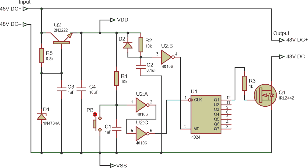
Figure 1’s circuit can flip on and flop off 48 VDC with a tiny push button. D1 is a 5.6-V Zener diode. It is connected to the base of the Q2 transistor. Its emitter voltage becomes around 5 VDC (VZ - VBE).
 |
|
| Figure 1. | The flip on, flop off circuit for 48 V. |
ICs U1 and U2 operate with this 5 VDC voltage. When the pushbutton (PB) is pushed once momentarily, a small pulse is generated, which is counted by U1. Its LSB pin becomes HIGH, which is applied to the gate of Q1. Hence, it conducts, and the output gets 48 VDC. For the next push of PB, the LSB pin of U1 goes LOW, and the gate of Q1 becomes LOW, and Q1 stops conducting. This makes the output voltage go to zero. This action repeats for every push.
Since PB encounters current around a milliamp, the low current, sleek PB is sufficient to switch ON or OFF the 48-V supply with high current. With a proper heatsink on Q1, this circuit can switch ON or OFF DC currents up to several amps as per the data sheet of Q1.
Both R1 and C1 are for PB switch debounce. Both R2 and C2 are for the power-on reset of U1.
One 20K resistor may be added between gate of Q1 and VSS (Ground).
Reference
- Woodward, Stephen. "Flip ON Flop OFF."