Kevin Tompsett, Analog Devices
EDN
Inexpensive boost regulators with on-chip FET power switches work well for low-voltage boost converters, SEPICs (single-ended primary-inductance converters), and flyback converters. For higher voltages, designers typically use a more expensive approach comprising a controller with an external FET or a high-voltage boost regulator.
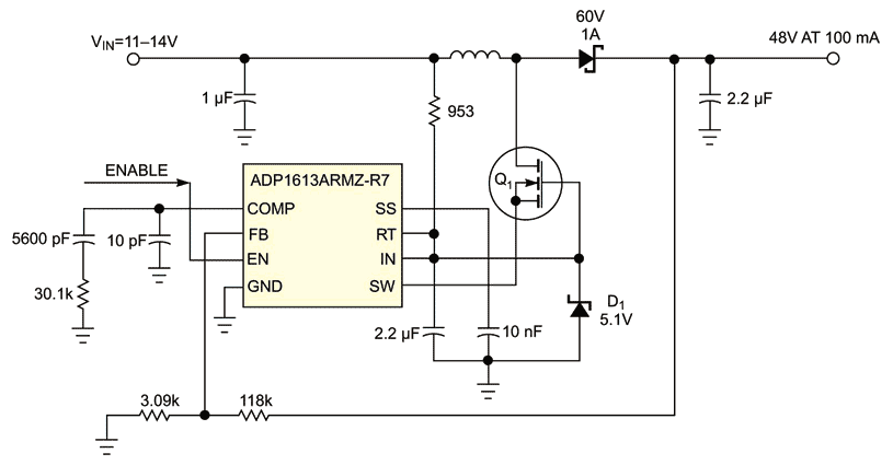
You can instead use an elegant and less expensive approach (Figure 1). The circuit uses an ADP1613 step-up dc/dc switching converter to produce a 48V, 100-mA supply, with 86% efficiency at full load (Figure 2). The IC includes an on-chip power switch that has 2A peak output currents at 20V. The zener diode acts as a shunt regulator that provides a 5V supply for the IC and biases the gate of the external FET at the same voltage. You connect the internal IC FET in series with a high-voltage FET, a cascode connection. The IC now drives the external FET in a common-gate mode, with the switching voltage at the source of the external FET instead of its gate.
 |
|
| Figure 1. | This circuit, designed using ADisimPower, uses the IC’s internal FET switch to drive the source of the external FET. |
 |
|
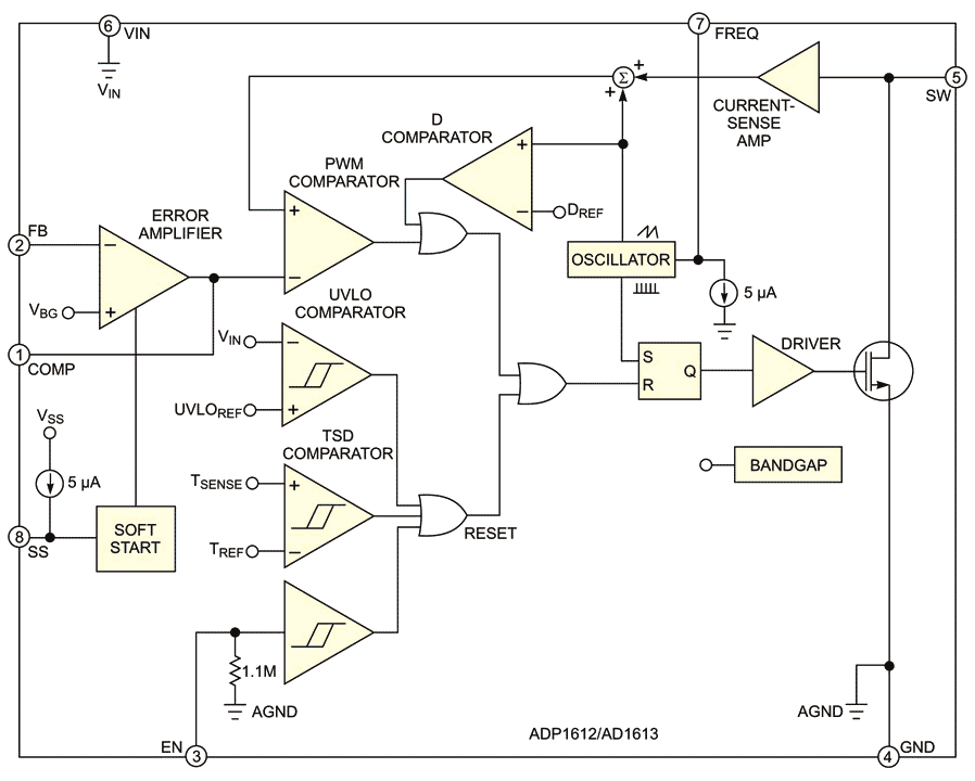
| Figure 2. | The IC’s block diagram shows its boost-converter architecture (courtesy Analog Devices). |
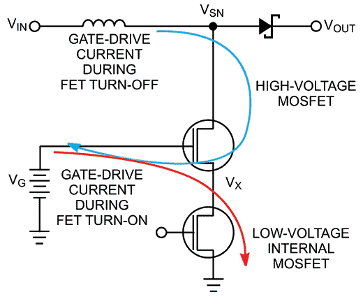
The internal FET then turns on, the VX node (Figure 3) is driven to ground, and the gate of the high-voltage FET remains constant, turning on the high-voltage FET. The lower FET acts like a low-resistance gate driver, and the FET quickly turns on, resulting in low turn-on loss. When the internal FET turns off, the inductor current pulls up the SW node until the external FET turns off. The highest voltage the internal FET will see is the gate voltage minus the threshold voltage of the external FET. The turn-off transition is slower because it is proportional to the peak current in the inductor, but, with a correctly sized FET, there is generally plenty of drive current for a fast transition and low loss, even at low load. The entire BOM cost is less than $2 (1000).
 |
|
| Figure 3. | The cascoded-FET arrangement results in fast switch transitions and low loss. The arrangement also enables higher-voltage operation. |
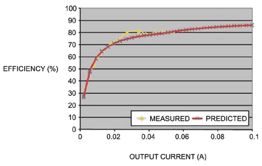
You can design and simulate this circuit using the ADIsimPower design tool, which is available at www.analog.com/adisimpower. The tool lets you design boost, SEPIC, and SEPIC-Cuk converters using this technique and allows input voltages of 1.8 to 90V and output voltages of 1.2 to 90V. Figure 4 shows good agreement between the ADIsimPower tool and the measured results, in terms of efficiency.
 |
|
| Figure 4. | The measured versus ADIsimPower results agree well. |
